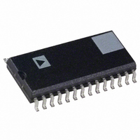
AD7708BRZ Analog Devices Inc, AD7708BRZ Datasheet - Page 12

AD7708BRZ
Manufacturer Part Number
AD7708BRZ
Description
IC ADC 16BIT R-R 8/10CH 28SOIC
Manufacturer
Analog Devices Inc
Datasheet
1.AD7708BRUZ-REEL.pdf
(44 pages)
Specifications of AD7708BRZ
Data Interface
DSP, MICROWIRE™, QSPI™, Serial, SPI™
Number Of Bits
16
Sampling Rate (per Second)
1.37k
Number Of Converters
1
Power Dissipation (max)
3.84mW
Voltage Supply Source
Analog and Digital
Operating Temperature
-40°C ~ 85°C
Mounting Type
Surface Mount
Package / Case
28-SOIC (0.300", 7.50mm Width)
Resolution (bits)
16bit
Input Channel Type
Pseudo Differential
Supply Voltage Range - Analogue
2.7V To 3.6V, 4.75V To 5.25V
Supply Voltage Range - Digital
2.7V To
Sampling Rate
105Hz
Rohs Compliant
Yes
Lead Free Status / RoHS Status
Lead free / RoHS Compliant
For Use With
EVAL-AD7708EBZ - BOARD EVAL FOR AD7708
Lead Free Status / RoHS Status
Lead free / RoHS Compliant, Lead free / RoHS Compliant
Available stocks
Company
Part Number
Manufacturer
Quantity
Price
Part Number:
AD7708BRZ
Manufacturer:
ADI/亚德诺
Quantity:
20 000
AD7708/AD7718
Pin No
1
2
3
4
5
6
7
8
9
10
11
12
13
14
15
16
17
18
19
20
Mnemonic
AIN7
AIN8
AV
AGND
REFIN1(–)
REFIN1(+)
AIN1
AIN2
AIN3
AIN4
AIN5
AINCOM
REFIN2(+)/AIN9
REFIN2(–)/AIN10
AIN6
P2
AGND
P1
RESET
SCLK
DD
Function
Analog Input Channel 7. Programmable-gain analog input that can be used as a pseudo-
differential input when used with AINCOM, or as the positive input of a fully-differential input
pair when used with AIN8. (See ADC Control Register section.)
Analog Input Channel 8. Programmable-gain analog input that can be used as a pseudo-
differential input when used with AINCOM, or as the negative input of a fully-differential input
pair when used with AIN7. (See ADC Control Register section.)
Analog Supply Voltage
Analog Ground
Negative Reference Input. This reference input can lie anywhere between AGND and AV
Positive reference input. REFIN(+) can lie anywhere between AV
reference voltage [REFIN(+)–REFIN(–)] is 2.5 V but the part is functional with a reference
range from 1 V to AV
Analog Input Channel 1. Programmable-gain analog input that can be used as a pseudo-
differential input when used with AINCOM, or as the positive input of a fully-differential input
pair when used with AIN2. (See ADC Control Register Section.)
Analog Input Channel 2. Programmable-gain analog input that can be used as a pseudo-
differential input when used with AINCOM, or as the negative input of a fully-differential input
pair when used with AIN1. (See ADC Control Register section.)
Analog Input Channel 3. Programmable-gain analog input that can be used as a pseudo-
differential input when used with AINCOM, or as the positive input of a fully-differential input
pair when used with AIN4. (See ADC Control Register section.)
Analog Input Channel 4. Programmable-gain analog input that can be used as a pseudo-
differential input when used with AINCOM, or as the negative input of a fully-differential input
pair when used with AIN3. (See ADC Control Register section.)
Analog Input Channel 5. Programmable-gain analog input that can be used as a pseudo-
differential input when used with AINCOM, or as the positive input of a fully-differential input
pair when used with AIN6. (See ADC Control Register section ADCCON.)
All analog inputs are referenced to this input when configured in pseudo-differential input mode.
Positive reference input/analog input. This input can be configured as a reference input with the
same characteristics as REFIN1(+) or as an additional analog input. When configured as an
analog input this pin provides a programmable-gain analog input that can be used as a pseudo-
differential input when used with AINCOM, or as the positive input of a fully-differential input
pair when used with AIN10. (See ADC Control Register section.)
Negative reference input/analog input. This pin can be configured as a reference or analog input.
When configured as a reference input it provides the negative reference input for REFIN2.
When configured as an analog input it provides a programmable-gain analog input that can be
used as a pseudo-differential input when used with AINCOM, or as the negative input of a fully-
differential input pair when used with AIN9. (See ADC Control Register section.)
Analog Input Channel 6. Programmable-gain analog input that can be used as a pseudo-
differential input when used with AINCOM, or as the negative input of a fully-differential input
pair when used with AIN5. (See ADC Control Register section.)
P2 can act as a general-purpose Input/Output bit referenced between AV
is a weak pull-up to AV
It is recommended that this pin be tied directly to AGND.
P1 can act as a general-purpose Input/Output bit referenced between AV
is a weak pull-up to AV
Digital input used to reset the ADC to its power-on-reset status. This pin has a weak pull-up
internally to DV
Serial clock input for data transfers to and from the ADC. The SCLK has a Schmitt-trigger
input making an opto-isolated interface more robust. The serial clock can be continuous with all
data transmitted in a continuous train of pulses. Alternatively, it can be a noncontinuous clock
with the information being transmitted to or from the AD7708/AD7718 in smaller batches of data.
PIN FUNCTION DESCRIPTIONS
DD
.
DD
DD
DD
.
internally on this pin.
internally on this pin.
DD
and AGND. The nominal
DD
DD
and AGND. There
and AGND. There
DD
– 1 V.


