AD7466BRTZ-R2 Analog Devices Inc, AD7466BRTZ-R2 Datasheet - Page 12
AD7466BRTZ-R2
Manufacturer Part Number
AD7466BRTZ-R2
Description
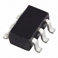
IC ADC 12BIT 1.6V LP SOT23-6
Manufacturer
Analog Devices Inc
Specifications of AD7466BRTZ-R2
Data Interface
DSP, MICROWIRE™, QSPI™, Serial, SPI™
Design Resources
Software Calibrated, 50 MHz to 9 GHz, RF Power Measurement System (CN0178)
Number Of Bits
12
Sampling Rate (per Second)
200k
Number Of Converters
1
Power Dissipation (max)
900µW
Voltage Supply Source
Single Supply
Operating Temperature
-40°C ~ 85°C
Mounting Type
Surface Mount
Package / Case
SOT-23-6
Resolution (bits)
12bit
Sampling Rate
200kSPS
Input Channel Type
Single Ended
Supply Voltage Range - Analog
1.6V To 3.6V
Supply Current
300µA
Lead Free Status / RoHS Status
Lead free / RoHS Compliant
For Use With
EVAL-AD7466CBZ - BOARD EVALUATION FOR AD7466
Lead Free Status / RoHS Status
Lead free / RoHS Compliant, Lead free / RoHS Compliant
Available stocks
Company
Part Number
Manufacturer
Quantity
Price

Part Number:
AD7466BRTZ-R2
Manufacturer:
ADI/亚德诺
Quantity:
20 000


AD7466/AD7467/AD7468
PIN CONFIGURATIONS AND FUNCTION DESCRIPTIONS
Table 6. Pin Function Descriptions
SOT-23
6
1
2
3
5
4
Pin No.
MSOP
1
8
7
6
2
3
4, 5
Figure 4. SOT-23 Pin Configuration
GND
V
V
DD
IN
Mnemonic
CS
V
GND
V
SDATA
SCLK
NC
1
2
3
DD
IN
(Not to Scale)
AD7466/
AD7467/
AD7468
TOP VIEW
Description
Chip Select. Active low logic input. This input provides the dual function of initiating conversions on the
devices and frames the serial data transfer.
Power Supply Input. The V
Analog Ground. Ground reference point for all circuitry on the devices. All analog input signals should
be referred to this GND voltage.
Analog Input. Single-ended analog input channel. The input range is 0 V to V
Data Out. Logic output. The conversion result from the AD7466/AD7467/AD7468 is provided on this
output as a serial data stream. The bits are clocked out on the falling edge of the SCLK input. The data
stream from the AD7466 consists of four leading zeros followed by the 12 bits of conversion data,
provided MSB first. The data stream from the AD7467 consists of four leading zeros followed by the 10
bits of conversion data, provided MSB first. The data stream from the AD7468 consists of four leading
zeros followed by the 8 bits of conversion data, provided MSB first.
Serial Clock. Logic input. SCLK provides the serial clock for accessing data from the parts. This clock
input is also used as the clock source for the conversion process of the parts.
No Connect.
6
5
4
CS
SDATA
SCLK
Rev. C | Page 12 of 28
DD
range for the devices is from 1.6 V to 3.6 V.
SDATA
Figure 5. MSOP Pin Configuration
SCLK
NC
CS
1
2
3
4
NC = NO CONNECT
(Not to Scale)
AD7466/
AD7467/
AD7468
TOP VIEW
DD
8
7
6
5
.
V
GND
V
NC
DD
IN
Related parts for AD7466BRTZ-R2
Image
Part Number
Description
Manufacturer
Datasheet
Request
R

Part Number:
Description:
Dual Precision, 500 ns Settling, BiFET Op Amp
Manufacturer:
Analog Devices
Datasheet:

Part Number:
Description:
±1.7g Dual-Axis IMEMS Accelerometer Evaluation Board
Manufacturer:
Analog Devices Inc
Datasheet:

Part Number:
Description:
Inertial Sensor Evaluation System
Manufacturer:
Analog Devices Inc
Datasheet:
Part Number:
Description:
Manufacturer:
Analog Devices Inc
Datasheet:
Part Number:
Description:
Manufacturer:
Analog Devices Inc
Datasheet:
Part Number:
Description:
Manufacturer:
Analog Devices Inc
Datasheet:
Part Number:
Description:
Manufacturer:
Analog Devices Inc
Datasheet:
Part Number:
Description:
Manufacturer:
Analog Devices Inc
Datasheet:
Part Number:
Description:
Manufacturer:
Analog Devices Inc
Datasheet:
Part Number:
Description:
Manufacturer:
Analog Devices Inc
Datasheet:
Part Number:
Description:
Manufacturer:
Analog Devices Inc
Datasheet:
Part Number:
Description:
Manufacturer:
Analog Devices Inc
Datasheet:
Part Number:
Description:
Manufacturer:
Analog Devices Inc
Datasheet: