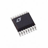
LTC2440IGN#PBF Linear Technology, LTC2440IGN#PBF Datasheet - Page 21

LTC2440IGN#PBF
Manufacturer Part Number
LTC2440IGN#PBF
Description
IC ADC DIFFER 24-BIT HS 16-SSOP
Manufacturer
Linear Technology
Datasheet
1.LTC2440CGN.pdf
(28 pages)
Specifications of LTC2440IGN#PBF
Number Of Bits
24
Sampling Rate (per Second)
3.5k
Data Interface
MICROWIRE™, Serial, SPI™
Number Of Converters
2
Power Dissipation (max)
40mW
Voltage Supply Source
Single Supply
Operating Temperature
-40°C ~ 85°C
Mounting Type
Surface Mount
Package / Case
16-SSOP (0.150", 3.90mm Width)
Lead Free Status / RoHS Status
Lead free / RoHS Compliant
Available stocks
Company
Part Number
Manufacturer
Quantity
Price
APPLICATIONS INFORMATION
The sample rate f
driving the f
rate is f
clock applied to f
sample rate leads to notch frequencies f
maintaining simple antialiasing requirements. A 100kHz
clock applied to f
harmonics up to 20kHz, see Figure 14. This is useful in
applications requiring digitalization of the DC component
of a noisy input signal and eliminates the need of placing
a 0.6Hz fi lter in front of the ADC.
An external oscillator operating from 100kHz to 20MHz can
be implemented using the LTC1799 (resistor set SOT-23
oscillator), see Figure 22. By fl oating pin 4 (DIV) of the
LTC1799, the output oscillator frequency is:
The normal mode rejection characteristic shown in Fig-
ure 14 is achieved by applying the output of the LTC1799
(with R
tied HIGH (OSR = 32768).
f
OSC
SET
S
=
= f
10
= 100k) to the f
O
EOSC
MHz
pin with an external oscillator. The sample
O
/5, where f
S
. Combining a large OSR with a reduced
O
•
and NULL f
⎛
⎜
⎝
results in a NULL at 0.6Hz plus all
10
10
•
R
k
SET
O
pin on the LTC2440 with SDI
EOSC
⎞
⎟
⎠
N
, my also be adjusted by
is the frequency of the
–120
–140
–100
Figure 14. LTC2440 Normal Mode Rejection
(External Oscillator at 90kHz)
–20
–40
–60
–80
N
0
near DC while
0
DIFFERENTIAL INPUT SIGNAL FREQUENCY (Hz)
2
4
6
Reduced Power Operation
In addition to adjusting the speed/resolution of the
LTC2440, the speed/resolution/power dissipation may
also be adjusted using the automatic sleep mode. During
the conversion cycle, the LTC2440 draws 8mA supply
current independent of the programmed speed. Once the
conversion cycle is completed, the device automatically
enters a low power sleep state drawing 8μA. The device
remains in this state as long as CS is HIGH and data is not
shifted out. By adjusting the duration of the sleep state
(hold CS HIGH longer) and the duration of the conversion
cycle (programming OSR) the DC power dissipation can
be reduced, see Figure 16.
For example, if the OSR is programmed at the fastest rate
(OSR = 64, t
the effective output rate is approximately 100Hz while the
average supply current is reduced to 240μA. By further
extending the sleep state to 100ms, the effective output
rate of 10Hz draws on average 30μA. Noise, power, and
speed can be optimized by adjusting the OSR (Noise/Speed)
and sleep mode duration (Power).
8
2440 F14
10
CONV
= 0.285ms) and the sleep state is 10ms,
LTC2440
21
2440fd


