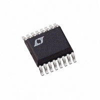
LTC2440IGN#PBF Linear Technology, LTC2440IGN#PBF Datasheet - Page 19

LTC2440IGN#PBF
Manufacturer Part Number
LTC2440IGN#PBF
Description
IC ADC DIFFER 24-BIT HS 16-SSOP
Manufacturer
Linear Technology
Datasheet
1.LTC2440CGN.pdf
(28 pages)
Specifications of LTC2440IGN#PBF
Number Of Bits
24
Sampling Rate (per Second)
3.5k
Data Interface
MICROWIRE™, Serial, SPI™
Number Of Converters
2
Power Dissipation (max)
40mW
Voltage Supply Source
Single Supply
Operating Temperature
-40°C ~ 85°C
Mounting Type
Surface Mount
Package / Case
16-SSOP (0.150", 3.90mm Width)
Lead Free Status / RoHS Status
Lead free / RoHS Compliant
Available stocks
Company
Part Number
Manufacturer
Quantity
Price
APPLICATIONS INFORMATION
falling edge of SCK. The internally generated serial clock
is output to the SCK pin. This signal may be used to shift
the conversion result into external circuitry. EOC can be
latched on the fi rst rising edge of SCK and the last bit of
the conversion result can be latched on the 32nd rising
edge of SCK. After the 32nd rising edge, SDO goes HIGH
(EOC = 1) indicating a new conversion is in progress. SCK
remains HIGH during the conversion.
Normal Mode Rejection and Antialiasing
One of the advantages delta-sigma ADCs offer over
conventional ADCs is on-chip digital fi ltering. Combined
with a large oversampling ratio, the LTC2440 signifi cantly
simplifi es antialiasing fi lter requirements.
The LTC2440’s speed/resolution is determined by the
over sample ratio (OSR) of the on-chip digital fi lter. The
OSR ranges from 64 for 3.5kHz output rate to 32,768
for 6.9Hz output rate. The value of OSR and the sample
rate f
The fi rst NULL of the digital fi lter is at f
of f
N
(INTERNAL)
S
where f
determine the fi lter characteristics of the device.
BUSY
SDO
SCK
CS
N
= f
CONVERSION
S
/OSR, see Figure 11 and Table 5. The
BIT 31
EOC
SLEEP
BIT 30
Figure 10. Internal Serial Clock, Continuous Operation
ANALOG INPUT RANGE
REFERENCE VOLTAGE
–0.5V
N
BIT 29
SIG
and multiples
REF
0.1V TO V
TO 0.5V
BIT 28
MSB
1μF
4.5V TO 5.5V
REF
CC
1, 8, 9, 16
2
3
4
5
6
BIT 27
V
REF
REF
IN
IN
GND
CC
+
–
LTC2440
+
–
DATA OUTPUT
rejection at the frequency f
see Figure 12.
If f
1.8MHz ±5% (over supply and temperature variations). At
an OSR of 32,768, the fi rst NULL is at f
no latency output rate is f
Figure 11. LTC2440 Normal Mode Rejection (Internal Oscillator)
BUSY
BIT 26
SDO
SCK
EXT
SDI
O
CS
f
O
is grounded, f
15
14
13
12
11
7
10
V
CC
–100
–120
–140
2-WIRE
SPI INTERFACE
–20
–40
–60
–80
V
CC
0
= EXTERNAL OSCILLATOR
= INTERNAL OSCILLATOR
200nV NOISE, 50/60Hz REJECTION
10-SPEED/RESOLUTION PROGRAMMABLE
2μV NOISE, 880Hz OUTPUT RATE
0
DIFFERENTIAL INPUT SIGNAL FREQUENCY (Hz)
LSB
BIT 5
24
S
60
is set by the on-chip oscillator at
N
N
/ 8 = 6.9Hz. At the maximum
120
±14% is better than 80dB,
BIT 0
180
LTC2440
N
CONVERSION
= 55Hz and the
2440 F11
240
2410 F10
19
2440fd


