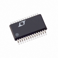
LTC1405IGN Linear Technology, LTC1405IGN Datasheet - Page 3

LTC1405IGN
Manufacturer Part Number
LTC1405IGN
Description
IC ADC 12BIT 5MSPS SAMPLE 28SSOP
Manufacturer
Linear Technology
Datasheet
1.LTC1405IGNPBF.pdf
(20 pages)
Specifications of LTC1405IGN
Number Of Bits
12
Sampling Rate (per Second)
5M
Data Interface
Parallel
Number Of Converters
1
Power Dissipation (max)
145mW
Voltage Supply Source
Dual ±
Operating Temperature
-40°C ~ 85°C
Mounting Type
Surface Mount
Package / Case
28-SSOP (0.150", 3.95mm Width)
Lead Free Status / RoHS Status
Contains lead / RoHS non-compliant
Available stocks
Company
Part Number
Manufacturer
Quantity
Price
Part Number:
LTC1405IGN
Manufacturer:
LINEAR/凌特
Quantity:
20 000
Company:
Part Number:
LTC1405IGN#PBF
Manufacturer:
Linear Technology
Quantity:
135
Part Number:
LTC1405IGN#PBF
Manufacturer:
LINEAR/凌特
Quantity:
20 000
Part Number:
LTC1405IGN#TRPBF
Manufacturer:
LINEAR/凌特
Quantity:
20 000
I TER AL REFERE CE CHARACTERISTICS
DIGITAL I PUTS AND OUTPUTS
A
specifications are at T
SYMBOL
t
t
CMRR
DY
otherwise specifications are at T
– A
SYMBOL
S/(N + D)
THD
SFDR
IMD
T
PARAMETER
V
V
V
V
V
V
temperature range, otherwise specifications are at T
operation. (Note 5)
SYMBOL
V
V
AP
jitter
U
A
CM
CM
CM
CM
REF
REF
IH
IL
U
IN
= 25°C. Specifications are guaranteed for both dual supply and single supply operation. (Note 5)
Output Voltage
Output Tempco
Line Regulation
Output Resistance
Output Voltage
Output Tempco
U W
= 0V. (Note 6)
A
A
LOG
U
PARAMETER
Sample-and-Hold Aperture Delay Time
Sample-and-Hold Aperture Delay Time Jitter
Analog Input Common Mode Rejection Ratio
PARAMETER
Signal-to-Noise Plus Distortion Ratio
Total Harmonic Distortion
Peak Harmonic or Spurious Noise
Intermodulation Distortion
Full-Power Bandwidth
Input Referred Noise
PARAMETER
High Level Input Voltage (Clock Pin)
Low Level Input Voltage (Clock Pin)
IC
U
I
ACCURACY
U
A
PUT
= 25°C. Specifications are guaranteed for both dual supply and single supply operation. (Note 5)
The
A
U
U
= 25°C. V
●
denotes the specifications which apply over the full operating temperature range, otherwise
The
DD
●
= 5V, V
denotes the specifications which apply over the full operating temperature range,
CONDITIONS
1MHz Input Signal
2.5MHz Input Signal
1MHz Input Signal, First 5 Harmonics
2.5MHz Input Signal, First 5 Harmonics
1MHz Input Signal
2.5MHz Input Signal
f
±2.048V Input Range
±1.024V Input Range, 2x Mode (SENSE = GAIN = 0V)
IN1
= 29.37kHz, f
A
CONDITIONS
–2.048V < (–A
CONDITIONS
I
I
4.75V ≤ V
– 5.25V ≤ V
0.1mA ≤
SENSE = GND, I
SENSE = V
SENSE = V
CONDITIONS
V
V
V
V
OUT
OUT
SS
DD
DD
DD
DD
= 25°C. Specifications are guaranteed for both dual supply and single supply
= – 5V, f
= 5.25V, V
= 5.25V, V
= 4.75V, V
= 4.75V, V
= 0
= 0
⏐
The
DD
I
REF
DD
OUT
SS
IN2
≤ 5.25V
SAMPLE
, I
IN
≤ –4.75V
●
⏐
SS
SS
SS
SS
= 32.446kHz
OUT
OUT
= +A
≤ 0.1mA
denotes the specifications which apply over the full operating
= 0V
= – 5V
= 0V
= – 5V
= 0
= 0
IN
= 5MHz, V
) < 2.048V
REF
= 4.096V. + A
●
●
●
●
●
●
●
●
●
●
IN
2.475
= – 0.1dBFS single ended input,
69.0
68.7
MIN
MIN
MIN
MIN
2.4
3.5
External Reference
Drive V
2.500
4.096
2.048
– 250
71.6
71.3
0.22
0.33
0.03
TYP
TYP
– 87
– 83
– 89
– 85
– 80
TYP
100
±15
±15
TYP
0.6
0.6
75
8
REF
LTC1405
with
– 78.5
– 77.0
– 79.5
– 78.0
2.525
MAX
MAX
MAX
MAX
0.8
1
LSB
LSB
ppm/°C
ppm/°C
UNITS
UNITS
UNITS
UNITS
mV/V
mV/V
1405fa
3
MHz
RMS
RMS
dB
dB
dB
dB
dB
dB
dB
dB
ps
ps
Ω
V
V
V
V
V
V
V
V


