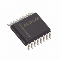
MAX194BEWE+ Maxim Integrated Products, MAX194BEWE+ Datasheet - Page 8

MAX194BEWE+
Manufacturer Part Number
MAX194BEWE+
Description
IC ADC 14BIT 85KSPS 16-SOIC
Manufacturer
Maxim Integrated Products
Datasheet
1.MAX194BEWE.pdf
(24 pages)
Specifications of MAX194BEWE+
Number Of Bits
14
Sampling Rate (per Second)
85k
Data Interface
QSPI™, Serial, SPI™
Number Of Converters
1
Power Dissipation (max)
80mW
Voltage Supply Source
Analog and Digital, Dual ±
Operating Temperature
-40°C ~ 85°C
Mounting Type
Surface Mount
Package / Case
16-SOIC (0.300", 7.50mm Width)
Conversion Rate
85 KSPs
Resolution
14 bit
Maximum Operating Temperature
+ 85 C
Mounting Style
SMD/SMT
Input Voltage
5 V
Minimum Operating Temperature
- 40 C
Lead Free Status / RoHS Status
Lead free / RoHS Compliant
14-Bit, 85ksps ADC with 10µA Shutdown
SPI/QSPI are trademarks of Motorola Corp.
8
Figure 4. Initiating Conversions—Less than 3 CLK cycles since end of previous conversion.
sion and EOC will go high on the following CLK falling
edge (Figure 4). CONV is ignored during conversions.
The conversion clock (CLK) should have a duty cycle
between 25% and 75% at 1.7MHz (the maximum clock
frequency). For lower frequency clocks, ensure the
minimum high and low times exceed 150ns. The mini-
mum clock rate for accurate conversion is 125Hz for
temperatures up to +70°C or 1kHz at +125°C due to
leakage of the sampling capacitor array. In addition,
CLK should not remain high longer than 50ms at tem-
peratures up to +70°C or 500µs at +125°C. If CLK is
held high longer than this, RESET must be pulsed low
to initiate a recalibration because it is possible that
state information stored in internal dynamic memory
may be lost. The MAX194’s clock can be stopped
indefinitely if it is held low.
If the frequency, duty cycle, or other aspects of the
clock signal’s shape change, the offset created by cou-
pling between CLK and the analog inputs (AIN and
REF) changes. Recalibration corrects for this offset and
restores DC accuracy.
_______________________________________________________________________________________
TRACK/HOLD
CONV
CLK
EOC
t
CC1
CONVERSION
ENDS
*
External Clock
t
CC2
t
CW
*
THE FALLING EDGE OF CONV MUST OCCUR IN THIS REGION
t
CEL
t
AQ
The conversion result is clocked out MSB first, format-
ted as 14 data bits plus two sub-LSBs. Serial data is
available on DOUT only when CS is held low.
Otherwise, DOUT is in a high-impedance state. There
are two ways to read the data on DOUT. To read the
data bits as they are determined (at the CLK clock
rate), hold CS low during the conversion. To read
results between conversions, hold CS low and clock
SCLK at up to 5MHz.
If you read the serial data bits as they are determined
(at the conversion-clock rate), EOC frames the data bits
(Figure 6). Conversion begins with the first falling CLK
edge, after CONV goes low and the input signal has
been acquired. Data bits are shifted out of DOUT on
subsequent falling CLK edges. Clock data in on CLK’s
rising edge or, if the clock speed is greater than 1MHz,
on the following falling edge of CLK to meet the maxi-
mum CLK-to-DOUT timing specification. See the
Operating Modes and SPI™/QSPI™ Interfaces section
for additional information. Reading the serial data dur-
ing the conversion results in the maximum conversion
throughput, because a new conversion can begin
immediately after the input acquisition period following
the previous conversion.
CONVERSION
BEGINS
t
CEH
Output Data


