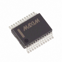
MAX113CAG+ Maxim Integrated Products, MAX113CAG+ Datasheet - Page 11

MAX113CAG+
Manufacturer Part Number
MAX113CAG+
Description
IC ADC 8BIT 400KSPS 24-SSOP
Manufacturer
Maxim Integrated Products
Datasheet
1.MAX113CAG.pdf
(12 pages)
Specifications of MAX113CAG+
Number Of Bits
8
Sampling Rate (per Second)
400k
Data Interface
Parallel
Number Of Converters
3
Power Dissipation (max)
640mW
Voltage Supply Source
Single Supply
Operating Temperature
0°C ~ 70°C
Mounting Type
Surface Mount
Package / Case
24-SSOP
Lead Free Status / RoHS Status
Lead free / RoHS Compliant
If the analog input exceeds 50mV beyond the sup-
plies, limit the input current to no more than two
milliamperes, as excessive current will degrade the
conversion accuracy of the on channel.
The track/hold enters hold mode when a conversion
starts (RD low or WR low). INT goes low at the end of
the conversion, at which point the track/hold enters
track mode. The next conversion can start after the
minimum acquisition time, t
Figure 10 shows the MAX113/MAX117’s nominal trans-
fer function. Code transitions occur halfway between
successive-integer LSB values. Output coding is binary
with 1LSB = (V
The maximum sampling rate (f
MAX117 is achieved in write-read mode (t
and is calculated as follows:
where t
between write and read pulses, t
and t
Signal-to-noise plus distortion (SINAD) is the ratio of the
fundamental input frequency’s RMS amplitude to all
other ADC output signals. The output spectrum is limit-
ed to frequencies above DC and below one-half the
ADC sample rate.
ACQ
WR
f
f
f
= minimum acquisition time.
MAX
MAX
MAX
= the write pulse width, t
=
REF+
t
WR
600ns 800ns 300ns 450ns
465kHz
______________________________________________________________________________________
- V
+ t
Signal-to-Noise Ratio and
REF-
Effective Number of Bits
RD
ACQ
) / 256.
+ t
1
RI
.
1
MAX
+ t
RI
Conversion Rate
8-Bit ADCs with 1µA Power-Down
= RD to INT delay,
Transfer Function
) for the MAX113/
ACQ
RD
= the delay
RD
Track/Hold
< t
INTL
+3V, 400ksps, 4/8-Channel,
)
The theoretical minimum analog-to-digital noise is
caused by quantization error, and results directly from
the ADC’s resolution: SNR = (6.02N + 1.76)dB, where
N is the number of bits of resolution. Therefore, a per-
fect 8-bit ADC can do no better than 50dB.
The FFT Plot (see Typical Operating Characteristics )
shows the result of sampling a pure 30.27kHz sinusoid
at a 400kHz rate. This FFT plot of the output shows the
output level in various spectral bands.
The effective resolution (or “effective number of bits”)
the ADC provides can be measured by transposing the
equation that converts resolution to SNR: N = (SINAD -
1.76) / 6.02 (see Typical Operating Characteristics ).
Total harmonic distortion (THD) is the ratio of the RMS
sum of all harmonics of the input signal (in the frequen-
cy band above DC and below one-half the sample rate)
to the fundamental itself. This is expressed as:
where V
through V
harmonics.
Spurious-free dynamic range (SFDR) is the ratio of the
fundamental RMS amplitude to the amplitude of the
next largest spectral component (in the frequency band
above DC and below one-half the sample rate). Usually
the next largest spectral component occurs at some
harmonic of the input frequency. However, if the ADC is
exceptionally linear, it may occur only at a random
peak in the ADC’s noise floor. See the Signal-to-Noise
Ratio graph in Typical Operating Characteristics .
THD = 20log
1
N
is the fundamental RMS amplitude, and V
are the amplitudes of the 2nd through Nth
Spurious-Free Dynamic Range
Total Harmonic Distortion
V
2
2
V
3
2
V
1
V
4
2
...V
N
2
11
2


