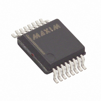
MAX1099CEAE+ Maxim Integrated Products, MAX1099CEAE+ Datasheet - Page 13

MAX1099CEAE+
Manufacturer Part Number
MAX1099CEAE+
Description
IC ADC 10BIT SERIAL 16-SSOP
Manufacturer
Maxim Integrated Products
Datasheet
1.MAX1099CEAE.pdf
(20 pages)
Specifications of MAX1099CEAE+
Number Of Bits
10
Sampling Rate (per Second)
900
Data Interface
MICROWIRE™, QSPI™, Serial, SPI™
Number Of Converters
1
Power Dissipation (max)
2.2mW
Voltage Supply Source
Single Supply
Operating Temperature
-40°C ~ 85°C
Mounting Type
Surface Mount
Package / Case
16-SSOP
Full Temp Accuracy
+/- 4 C
Digital Output - Bus Interface
Serial (3-Wire)
Digital Output - Number Of Bits
10 bit
Maximum Operating Temperature
+ 85 C
Minimum Operating Temperature
- 40 C
Output Type
Digital
Lead Free Status / RoHS Status
Lead free / RoHS Compliant
input sampling capacitance of the ADC (4pF). Source
impedances below 100kΩ have no significant effect on
MAX1098/MAX1099 AC performance.
Internal protection diodes clamp the analog inputs to
V
0.3V and V
accurate conversions, the inputs should not extend
beyond the supply rails.
If an off-channel analog input extends beyond the
supply rails, limit the input current to 2mA.
Figure 3a. Voltage Conversion Timing Diagram
Figure 3b. Temperature Conversion Timing Diagram
DD
SSTRB
SSTRB
and GND so channels can swing within GND -
FCLK
FCLK
DD
10-Bit Serial-Output Temperature Sensors
WARMUP
13 f
+ 0.3V without damage. However, for
_______________________________________________________________________________________
WARMUP
CLKs
13 f
CLKs
Analog Input Protection
CONVERSION CYCLE 1
ACQUISITION
INPUT
4 f
CLKs
ACQUISITION
CONVERSION CYCLE 1
FIRST CONVERSION
INPUT
F
CLKS
CYCLES 2–12
CONVERSION
REFERENCE
SAMPLING
44 f
CLKs
ACQUISITION 1
The MAX1098/MAX1099 feature a serial interface that is
fully compatible with SPI, QSPI, and MICROWIRE
devices. For SPI/QSPI, ensure that the CPU serial inter-
face runs in master mode so it generates the serial
clock signal. Select a 2.5MHz clock frequency or less,
and set zero values for clock polarity (CPOL) and
phase (CPHA) in the µP control registers. Figure 4
shows detailed serial interface timing information. See
Tables 1–4 for programming information.
REF
WARMUP
13 f
CONVERSION CYCLES 2–12
REFERENCE SAMPLING
CLKs
ACQUISITION 2
with 5-Channel ADC
REF
ACQUISITION
CONVERSION CYCLES 1–12
SECOND CONVERSION
INPUT
48 f
CLKs
Serial Digital Interface
WRITE TO OUTPUT
REGISTER
3 f
OUTPUT REGISTER
SUBTRACTION
AND WRITE TO
CLKs
3 f
CLKs
13


