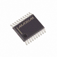
MAX1081BEUP+ Maxim Integrated Products, MAX1081BEUP+ Datasheet - Page 18

MAX1081BEUP+
Manufacturer Part Number
MAX1081BEUP+
Description
IC ADC 10BIT 300KSPS 20-TSSOP
Manufacturer
Maxim Integrated Products
Datasheet
1.MAX1080BEUP.pdf
(24 pages)
Specifications of MAX1081BEUP+
Number Of Bits
10
Sampling Rate (per Second)
300k
Data Interface
MICROWIRE™, QSPI™, Serial, SPI™
Number Of Converters
1
Power Dissipation (max)
8.0mW
Voltage Supply Source
Analog and Digital
Operating Temperature
-40°C ~ 85°C
Mounting Type
Surface Mount
Package / Case
20-TSSOP
Number Of Adc Inputs
8
Architecture
SAR
Conversion Rate
300 KSPs
Resolution
10 bit
Input Type
Differential
Interface Type
4-Wire (SPI, QSPI, MICROWIRE, TMS320)
Voltage Reference
Internal 2.5 V or External
Supply Voltage (max)
3.6 V
Supply Voltage (min)
2.7 V
Maximum Power Dissipation
559 mW
Maximum Operating Temperature
+ 85 C
Mounting Style
SMD/SMT
Minimum Operating Temperature
- 40 C
Lead Free Status / RoHS Status
Lead free / RoHS Compliant
300ksps/400ksps, Single-Supply, Low-Power,
8-Channel, Serial 10-Bit ADCs with Internal Reference
fast power-down (FASTPD) or reduced-power (REDP)
mode instead of in full power-up can further reduce
power consumption. This is achieved by using the
sequence shown in Figure 12a.
Figure 10b shows the MAX1081’s power consumption
for one- or eight-channel conversions utilizing FULLPD
mode (PD1 = PD0 = 0), an external reference, and the
maximum clock speed. One dummy conversion to
power up the device is needed, but no wait time is nec-
essary to start the second conversion, thereby achiev-
ing lower power consumption at up to half the full
sampling rate.
FASTPD and REDP modes achieve the lowest power
consumption at speeds close to the maximum sam-
pling rate. Figure 11 shows the MAX1081’s power con-
sumption in FASTPD mode (PD1 = 0, PD0 = 1), REDP
mode (PD1 = 1, PD0 = 0), and for comparison, normal
operating mode (PD1 = 1, PD0 = 1). The figure shows
power consumption using the specified power-down
mode, with the internal reference and conversion con-
Figure 12a. Full Power-Down Timing
Figure 12b. FASTPD and REDP Timing
18
Using Fast Power-Down and Reduced Power Modes
______________________________________________________________________________________
I
VDD1
REFADJ
+ I
VDD2
I
VDD1
DIN
REF
+ I
VDD2
DIN
REF
1
FULLPD
1
2.5mA
1.22V
2.5V
REDP
2.5V (ALWAYS ON)
0 0
2.5mA
1 0
0V
0V
0V
0.9mA
1
γ = RC = 17kΩ x 0.01µF
REDP
DUMMY CONVERSION
2.5mA
WAIT 1.4ms (7 x RC)
1
1 0
REDP
2.5mA
1.3mA OR 0.9mA
trolled at the maximum clock speed. The clock speed
in FASTPD or REDP should be limited to 4.8MHz for the
MAX1080/MAX1081. FULLPD mode may provide
increased power savings in applications where the
MAX1080/MAX1081 are inactive for long periods of
time, but intermittent bursts of high-speed conversions
are required. Figure 12b shows FASTPD and REDP tim-
ing.
The MAX1080/MAX1081 can be used with an internal
or external reference. An external reference can be
connected directly at REF or at the REFADJ pin.
An internal buffer is designed to provide 2.5V at
REF for the MAX1080/MAX1081. The internally trimmed
1.22V reference is buffered with a 2.05V/V gain.
The MAX1080/MAX1081s’ full-scale range with the inter-
nal reference is 2.5V with unipolar inputs and ±1.25V
with bipolar inputs. The internal reference voltage is
adjustable by ±100mV with the circuit in Figure 13.
1 0
0.9mA
1
Internal and External References
FULLPD
2.5mA
1.22V
2.5V
1
0 0
FASTPD
2.5mA
0mA
0 1
1.3mA
Internal Reference
1


