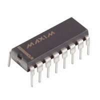
MAX1247BCPE+ Maxim Integrated Products, MAX1247BCPE+ Datasheet - Page 9

MAX1247BCPE+
Manufacturer Part Number
MAX1247BCPE+
Description
IC ADC SRL 4CH 12BIT 2.7V 16-DIP
Manufacturer
Maxim Integrated Products
Datasheet
1.MAX1247BCEE.pdf
(25 pages)
Specifications of MAX1247BCPE+
Number Of Bits
12
Sampling Rate (per Second)
133k
Data Interface
MICROWIRE™, QSPI™, Serial, SPI™
Number Of Converters
1
Power Dissipation (max)
842mW
Voltage Supply Source
Single Supply
Operating Temperature
0°C ~ 70°C
Mounting Type
Through Hole
Package / Case
16-DIP (0.300", 7.62mm)
Number Of Adc Inputs
4
Architecture
SAR
Conversion Rate
133 KSPs
Resolution
12 bit
Input Type
Voltage
Interface Type
4-Wire (SPI, QSPI, MICROWIRE, TMS320)
Supply Voltage (max)
5.25 V
Supply Voltage (min)
2.7 V
Maximum Power Dissipation
842 mW
Maximum Operating Temperature
+ 70 C
Mounting Style
SMD/SMT
Minimum Operating Temperature
0 C
Lead Free Status / RoHS Status
Lead free / RoHS Compliant
Figure 1. Load Circuits for Enable Time
______________________________________________________________Pin Description
DOUT
PIN
2–5
a) High-Z to V
10
11
12
13
14
15
16
1
6
7
8
9
6kΩ
OH
CH0–CH3
DGND
REFADJ
and V
SSTRB
NAME
DGND
AGND
SHDN
DOUT
SCLK
VREF
COM
V
DIN
CS
DD
OL
_______________________________________________________________________________________
to V
OH
C
50pF
LOAD
Positive Supply Voltage
Sampling Analog Inputs
Ground reference for analog inputs. COM sets zero-code voltage in single-ended mode. Must be
stable to ±0.5LSB.
Three-Level Shutdown Input. Pulling SHDN low shuts the MAX1246/MAX1247 down; otherwise, they
are fully operational. Pulling SHDN high puts the reference-buffer amplifier in internal compensation
mode. Letting SHDN float puts the reference-buffer amplifier in external compensation mode.
Reference-Buffer Output/ADC Reference Input. Reference voltage for analog-to-digital conversion.
In internal reference mode (MAX1246 only), the reference buffer provides a 2.500V nominal output,
externally adjustable at REFADJ. In external reference mode, disable the internal buffer by pulling
REFADJ to V
Input to the Reference-Buffer Amplifier. To disable the reference-buffer amplifier, tie REFADJ to V
Analog Ground
Digital Ground
Serial Data Output. Data is clocked out at SCLK’s falling edge. High impedance when CS is high.
Serial Strobe Output. In internal clock mode, SSTRB goes low when the MAX1246/MAX1247 begin the
A/D conversion, and goes high when the conversion is finished. In external clock mode, SSTRB pulses
high for one clock period before the MSB decision. High impedance when CS is high (external clock
mode).
Serial Data Input. Data is clocked in at SCLK’s rising edge.
Active-Low Chip Select. Data will not be clocked into DIN unless CS is low. When CS is high, DOUT is
high impedance.
Serial Clock Input. Clocks data in and out of serial interface. In external clock mode, SCLK also sets
the conversion speed. (Duty cycle must be 40% to 60%.)
b) High-Z to V
DOUT
DD
V
DD
OL
.
6kΩ
and V
C
DGND
50pF
LOAD
Serial 12-Bit ADCs in QSOP-16
+2.7V, Low-Power, 4-Channel,
OH
to V
OL
Figure 2. Load Circuits for Disable Time
FUNCTION
DOUT
6kΩ
a) V
OH
DGND
to High-Z
C
50pF
LOAD
DOUT
b) V
OL
V
to High-Z
DD
6kΩ
C
50pF
DGND
LOAD
DD
.
9


