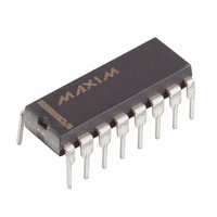
MAX1247BCPE+ Maxim Integrated Products, MAX1247BCPE+ Datasheet - Page 14

MAX1247BCPE+
Manufacturer Part Number
MAX1247BCPE+
Description
IC ADC SRL 4CH 12BIT 2.7V 16-DIP
Manufacturer
Maxim Integrated Products
Datasheet
1.MAX1247BCEE.pdf
(25 pages)
Specifications of MAX1247BCPE+
Number Of Bits
12
Sampling Rate (per Second)
133k
Data Interface
MICROWIRE™, QSPI™, Serial, SPI™
Number Of Converters
1
Power Dissipation (max)
842mW
Voltage Supply Source
Single Supply
Operating Temperature
0°C ~ 70°C
Mounting Type
Through Hole
Package / Case
16-DIP (0.300", 7.62mm)
Number Of Adc Inputs
4
Architecture
SAR
Conversion Rate
133 KSPs
Resolution
12 bit
Input Type
Voltage
Interface Type
4-Wire (SPI, QSPI, MICROWIRE, TMS320)
Supply Voltage (max)
5.25 V
Supply Voltage (min)
2.7 V
Maximum Power Dissipation
842 mW
Maximum Operating Temperature
+ 70 C
Mounting Style
SMD/SMT
Minimum Operating Temperature
0 C
Lead Free Status / RoHS Status
Lead free / RoHS Compliant
conversion already in progress. When internal clock
mode is selected, SSTRB does not go into a high-
impedance state when CS goes high.
Figure 9 shows the SSTRB timing in internal clock
mode. In this mode, data can be shifted in and out of
the MAX1246/MAX1247 at clock rates exceeding
2.0MHz if the minimum acquisition time (t
above 1.5µs.
The falling edge of CS does not start a conversion.
The first logic high clocked into DIN is interpreted as a
start bit and defines the first bit of the control byte. A
+2.7V, Low-Power, 4-Channel,
Serial 12-Bit ADCs in QSOP-16
Figure 7. External Clock Mode SSTRB Detailed Timing
Figure 8. Internal Clock Mode Timing
14
______________________________________________________________________________________
SSTRB
SCLK
SSTRB
DOUT
A/D STATE
SCLK
CS
DIN
CS
START
1
SEL2 SEL1 SEL0
2
3
IDLE
4
t
SDV
UNI/
BIP
•
5
• • •
• • •
• • •
SGL/
DIF
(f
ACQUISITION
SCLK
6
Data Framing
1.5µs
PD1
= 2MHz)
7
ACQ
PD0
8
(SHDN = FLOAT)
) is kept
CONVERSION
7.5µs MAX
PD0 CLOCKED IN
t
CONV
9
conversion starts on SCLK’s falling edge, after the eighth
bit of the control byte (the PD0 bit) is clocked into DIN.
The start bit is defined as follows:
If CS is toggled before the current conversion is com-
plete, the next high bit clocked into DIN is recognized as
a start bit; the current conversion is terminated, and a
new one is started.
MSB B10
B11
IDLE
10
The first high bit clocked into DIN with CS low any
time the converter is idle; e.g., after V
The first high bit clocked into DIN after bit 5 of a con-
version in progress is clocked onto the DOUT pin.
t
SSTRB
11
B9
12
18
B2
19
• • •
t
SSTRB
• • • •
• • •
B1
20
LSB
B0
OR
21
FILLED WITH
ZEROS
22
23
24
DD
t
STR
is applied.


