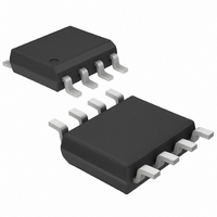
MAX1241BCSA+ Maxim Integrated Products, MAX1241BCSA+ Datasheet - Page 12

MAX1241BCSA+
Manufacturer Part Number
MAX1241BCSA+
Description
IC ADC SERIAL 12BIT 2.7V 8-SOIC
Manufacturer
Maxim Integrated Products
Datasheet
1.MAX1241BCSA.pdf
(15 pages)
Specifications of MAX1241BCSA+
Number Of Bits
12
Sampling Rate (per Second)
73k
Data Interface
MICROWIRE™, QSPI™, Serial, SPI™
Number Of Converters
1
Power Dissipation (max)
471mW
Voltage Supply Source
Single Supply
Operating Temperature
0°C ~ 70°C
Mounting Type
Surface Mount
Package / Case
8-SOIC (0.154", 3.90mm Width)
Number Of Adc Inputs
1
Architecture
SAR
Conversion Rate
73 KSPs
Resolution
12 bit
Input Type
Voltage
Voltage Reference
External
Supply Voltage (max)
5.25 V
Supply Voltage (min)
2.7 V
Maximum Power Dissipation
471 mW
Maximum Operating Temperature
+ 70 C
Mounting Style
SMD/SMT
Minimum Operating Temperature
0 C
Lead Free Status / RoHS Status
Lead free / RoHS Compliant
+2.7V, Low-Power,
12-Bit Serial ADCs in 8-Pin SO
5) With CS = high, wait the minimum specified time, t
CS must be held low until all data bits are clocked out.
Data can be output in two bytes or continuously, as
shown in Figure 8. The bytes contain the result of the
conversion padded with one leading 1, and trailing 0s.
When using SPI or MICROWIRE, set CPOL = 0 and
CPHA = 0. Conversion begins with a CS falling edge.
DOUT goes low, indicating a conversion in progress. Wait
until DOUT goes high or until the maximum specified
7.5µs conversion time elapses. Two consecutive 1-byte
reads are required to get the full 12 bits from the ADC.
DOUT output data transitions on SCLK’s falling edge and
is clocked into the µP on SCLK’s rising edge.
The first byte contains a leading 1, and seven bits of con-
version result. The second byte contains the remaining
five bits and three trailing zeros. See Figure 11 for con-
nections and Figure 12 for timing.
Set CPOL = CPHA = 0. Unlike SPI, which requires two
1-byte reads to acquire the 12 bits of data from the ADC,
QSPI allows the minimum number of clock cycles neces-
sary to clock in the data. The MAX1240/MAX1241
requires 13 clock cycles from the µP to clock out the 12
bits of data with no trailing zeros (Figure 13). The maxi-
mum clock frequency to ensure compatibility with QSPI is
2.097MHz.
For best performance, use printed circuit boards. Wire-
wrap boards are not recommended. Board layout should
ensure that digital and analog signal lines are separated
from each other. Do not run analog and digital (especially
clock) lines parallel to one another, or digital lines under-
neath the ADC package.
Figure 14 shows the recommended system ground con-
nections. Establish a single-point analog ground (“star”
ground point) at GND, separate from the logic ground.
Connect all other analog grounds and DGND to this star
ground point for further noise reduction. No other digital
12
before initiating a new conversion by pulling CS low.
If a conversion is aborted by pulling CS high before
the conversion’s end, wait for the minimum acquisi-
tion time, t
______________________________________________________________________________________
ACQ
Layout, Grounding, and Bypassing
, before starting a new conversion.
SPI and MICROWIRE
QSPI
CS
,
system ground should be connected to this single-point
analog ground. The ground return to the power supply for
this ground should be low impedance and as short as
possible for noise-free operation.
High-frequency noise in the V
the ADC’s high-speed comparator. Bypass this supply to
the single-point analog ground with 0.1µF and 4.7µF
bypass capacitors. Minimize capacitor lead lengths for
best supply-noise rejection. If the power supply is very
noisy, a 10Ω resistor can be connected as a lowpass filter
to attenuate supply noise (Figure 14).
Figure 11. Common Serial-Interface Connections to the
MAX1241
a) SPI
b) QSPI
c) MICROWIRE
MISO
MISO
SCK
SCK
I/O
SS
CS
SS
I/O
SK
SI
+3V
+3V
DD
power supply may affect
CS
SCLK
DOUT
CS
SCLK
DOUT
CS
SCLK
DOUT
MAX1240
MAX1241
MAX1240
MAX1241
MAX1240
MAX1241


