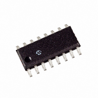
MCP3208-BI/SL Microchip Technology, MCP3208-BI/SL Datasheet - Page 20

MCP3208-BI/SL
Manufacturer Part Number
MCP3208-BI/SL
Description
IC ADC 12BIT 2.7V 8CH SPI 16SOIC
Manufacturer
Microchip Technology
Specifications of MCP3208-BI/SL
Number Of Converters
1
Package / Case
16-SOIC (0.154", 3.90mm Width)
Number Of Bits
12
Sampling Rate (per Second)
100k
Data Interface
Serial, SPI™
Voltage Supply Source
Single Supply
Operating Temperature
-40°C ~ 85°C
Mounting Type
Surface Mount
Architecture
SAR
Conversion Rate
100 KSPs
Resolution
12 bit
Input Type
Voltage
Snr
100 dB
Maximum Operating Temperature
+ 85 C
Mounting Style
SMD/SMT
Minimum Operating Temperature
- 40 C
Package
16SOIC N
Sampling Rate
100 KSPS
Number Of Adcs
1
Number Of Analog Inputs
8|4
Digital Interface Type
Serial (4-Wire, SPI)
Polarity Of Input Voltage
Unipolar
Lead Free Status / RoHS Status
Lead free / RoHS Compliant
Lead Free Status / RoHS Status
Lead free / RoHS Compliant, Lead free / RoHS Compliant
Available stocks
Company
Part Number
Manufacturer
Quantity
Price
Company:
Part Number:
MCP3208-BI/SL
Manufacturer:
MICROCHIP
Quantity:
12 000
Part Number:
MCP3208-BI/SL
Manufacturer:
MICROCHIP/微芯
Quantity:
20 000
MCP3204/3208
6.4
When laying out a printed circuit board for use with
analog components, care should be taken to reduce
noise wherever possible. A bypass capacitor should
always be used with this device, placed as close as
possible to the device pin. A bypass capacitor value of
1 µF is recommended.
Digital and analog traces should be separated as much
as possible on the board, with no traces running under-
neath the device or the bypass capacitor. Extra precau-
tions should be taken to keep traces with high
frequency signals (such as clock lines) as far as
possible from analog traces.
Use of an analog ground plane is recommended in
order to keep the ground potential the same for all
devices on the board. Providing V
devices in a “star” configuration can also reduce noise
by eliminating return current paths and associated
errors (see Figure 6-4). For more information on layout
tips when using A/D converters, refer to AN688,
“Layout Tips for 12-Bit A/D converter Applications”.
FIGURE 6-4:
‘Star’ configuration in order to reduce errors
caused by current return paths.
DS21298C-page 20
Device 1
Layout Considerations
Device 2
V
Connection
DD
V
traces arranged in a
DD
DD
Device 3
connections to
Device 4
6.5
The MCP3204/3208 devices provide both digital and
analog ground connections to provide another means
of noise reduction. As shown in Figure 6-5, the analog
and digital circuitry is separated internal to the device.
This reduces noise from the digital portion of the device
being coupled into the analog portion of the device. The
two grounds are connected internally through the sub-
strate, which has a resistance of 5 -10 .
If no ground plane is utilized, then both grounds must
be connected to V
available, both digital and analog ground pins should
be connected to the analog ground plane. If both an
analog and a digital ground plane are available, both
the digital and the analog ground pins should be con-
nected to the analog ground plane. Following these
steps will reduce the amount of digital noise from the
rest of the board being coupled into the A/D converter.
FIGURE 6-5:
Digital Ground Pins.
Digital Side
-SPI Interface
-Shift Register
-Control Logic
Utilizing the Digital and Analog
Ground Pins
DGND
Analog Ground Plane
SS
MCP3204/08
V
Substrate
on the board. If a ground plane is
5 - 10
DD
Separation of Analog and
2002 Microchip Technology Inc.
Analog Side
-Sample Cap
-Capacitor Array
-Comparator
AGND
0.1 µF


