MCP3550-50E/MS Microchip Technology, MCP3550-50E/MS Datasheet - Page 4

MCP3550-50E/MS
Manufacturer Part Number
MCP3550-50E/MS
Description
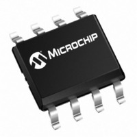
IC ADC 22BIT 2.7V 1CH 8MSOP
Manufacturer
Microchip Technology
Specifications of MCP3550-50E/MS
Data Interface
Serial, SPI™
Number Of Bits
22
Sampling Rate (per Second)
12.5
Number Of Converters
1
Voltage Supply Source
Single Supply
Operating Temperature
-40°C ~ 125°C
Mounting Type
Surface Mount
Package / Case
8-TSSOP, 8-MSOP (0.118", 3.00mm Width)
Resolution (bits)
22bit
Sampling Rate
12.5SPS
Input Channel Type
Differential
Supply Voltage Range - Analog
2.7V To 5.5V
Supply Current
120µA
Lead Free Status / RoHS Status
Lead free / RoHS Compliant
For Use With
MCP355XDV-MS1 - BOARD DEV SENSOR APP MCP355XMCP355XDM-TAS - BOARD DEMO TINY APP SNSR MCP355X
Lead Free Status / RoHS Status
Lead free / RoHS Compliant, Lead free / RoHS Compliant
MCP3550/1/3
DC CHARACTERISTICS (CONTINUED)
DS21950E-page 4
Electrical Specifications: Unless otherwise indicated, all parameters apply at -40°C ≤ T
V
applies to entire MCP3550/1/3 family.
Rejection Performance
Common Mode DC Rejection
Power Supply DC Rejection
Common Mode 50/60 Hz Rejection
Power Supply 50/60 Hz Rejection
Power Supply 50/60 Hz Rejection
Normal Mode 50 and 60 Hz
Rejection
Normal Mode 50 or 60 Hz
Rejection
Analog Inputs
Differential Input Range
Absolute/Common Mode Voltages
Analog Input Sampling Capacitor
Differential Input Impedance
Shutdown Mode Leakage Current
Reference Input
Voltage Range
Reference Input Sampling
Capacitor
Reference Input Impedance
Shutdown Mode Reference
Leakage Current
Power Requirements
Power Supply Voltage Range
MCP3550-50, MCP3551 Supply
Current
MCP3550-60, MCP3553 Supply
Current
Supply Current, Sleep Mode
Supply Current, Shutdown Mode
Serial Interface
Voltage Input High (CS, SCK)
Voltage Input Low (CS, SCK)
Voltage Output High (SDO/RDY)
Note 1:
REF
= 2.5V. V
2:
3:
4:
5:
6:
Parameters
This parameter is established by characterization and not 100% tested.
INL is the difference between the endpoints line and the measured code at the center of the quantization band.
This current is due to the leakage current and the current due to the offset voltage between V
Input impedance is inversely proportional to clock frequency; typical values are for the MCP3550/1 device. V
Characterized by design, but not tested.
Rejection performance depends on internal oscillator accuracy; see Section 4.0 “Device Overview” for more informa-
tion on oscillator and digital filter design. MCP3550/1 device rejection specifications characterized from 49 to 61 Hz.
IN
+ = V
IN
- = V
(1,6)
CM
= V
REF
V
IN+
/2. All ppm units use 2*V
CMRR
NMRR
NMRR
PSRR
PSRR
I
Sym
I
V
DDSL
V
V
I
I
DDS
V
DD
DD
DD
OH
− V
IH
IL
IN-
V
V
0.7 V
-V
SS
DD
Min
0.1
2.7
—
—
—
—
—
—
—
—
—
—
—
—
—
—
—
—
—
—
—
—
REF
- 0.3
- 0.5
DD
-135
-135
-120
-120
-115
Typ
120
100
140
120
-85
-85
2.4
2.4
REF
10
15
10
—
—
—
—
—
—
—
—
1
1
as full scale range. Unless otherwise noted, specification
V
DD
+V
Max
V
170
185
5.5
0.4
—
—
—
—
—
—
—
—
—
—
—
—
—
—
—
—
—
1
REF
+ 0.3
DD
Units
MΩ
MΩ
dB
dB
dB
dB
dB
dB
dB
nA
nA
µA
µA
µA
µA
µA
µA
pF
pF
V
V
V
V
V
V
V
A
≤ +85°C, V
V
V
MCP3551 only, V
4.5V to 5.5V
MCP3550-50 or MCP3550-60 only
at 50 or 60 Hz respectively, V
varies from 4.5V to 5.5V
MCP3551 only,
0 < V
-V
MCP3550-50 or MCP3550-60 only
at 50 or 60 Hz respectively,
0 < V
-V
Note 5
V
(Note 3)
Note 5
Note 4
V
V
V
V
V
CS = SCK = V
V
© 2009 Microchip Technology Inc.
CM
CM
IN
IN
DD
DD
DD
DD
OH
REF
REF
+ = V
+ = V
= 5V
= 2.7V
= 5V
= 2.7V
= 1 mA, V
range from 0 to V
varies from 0V to V
CM
CM
DD
< V
< V
= 2.7V or 5.0V.
< V
< V
IN
IN
IN
IN
IN
- = V
- = V
+ and V
Conditions
= (V
= (V
DD
DD
DD
,
,
DD
DD
SS
IN
IN
DD
; CS = V
; CS = V
= 5.0V
+ -V
+ -V
IN
varies from
-.
DD
IN
IN
DD
-) < +V
-) < +V
REF
DD
DD
= 5V.
DD
REF
REF


