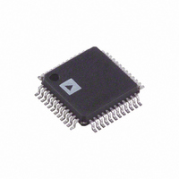
AD9875BST Analog Devices Inc, AD9875BST Datasheet - Page 24

AD9875BST
Manufacturer Part Number
AD9875BST
Description
IC 10BIT MODEM MXFE 48-LQFP
Manufacturer
Analog Devices Inc
Datasheet
1.AD9875BST.pdf
(28 pages)
Specifications of AD9875BST
Rohs Status
RoHS non-compliant
Number Of Bits
10
Number Of Channels
1
Power (watts)
950mW
Voltage - Supply, Analog
3V
Voltage - Supply, Digital
3.3V
Package / Case
48-LQFP
Main Category
Single Chip
Sub-category
Converter
Power Supply Type
Analog/Digital
Operating Supply Voltage (typ)
3.3V
Package Type
LQFP
Operating Supply Voltage (min)
3V
Operating Supply Voltage (max)
3.6V
Supply Current
262mA
Operating Temp Range
-40C to 85C
Operating Temperature Classification
Industrial
Pin Count
48
Mounting
Surface Mount
Lead Free Status / RoHS Status
Not Compliant
Available stocks
Company
Part Number
Manufacturer
Quantity
Price
Company:
Part Number:
AD9875BST
Manufacturer:
ADI
Quantity:
315
AD9875
The AVDD and DVDD power planes may be fed from the same
low noise voltage source; however, they should be decoupled from
each other to prevent the noise generated in the DVDD portion
of the MxFE from corrupting the AVDD supply. This can be done
by using ferrite beads between the voltage source and DVDD,
and between the source and AVDD. Both DVDD and AVDD
should have a low ESR, bulk decoupling capacitor on the MxFE
side of the ferrite as well as a low ESR, ESL decoupling capacitors
on each supply pin (i.e., the AD9875 requires five power supply
decoupling caps, one each on Pins 5, 38, 47, 14, and 35). The
decoupling caps should be placed as close to the MxFE supply
pins as possible. An example of the proper decoupling is shown
in the AD9875 evaluation board schematic.
Ground Planes
In general, if the component placing guidelines discussed earlier
can be implemented, it is best to have at least one continuous
ground plane for the entire board. All ground connections should
be made as short as possible. This will result in the lowest imped-
ance return paths, and the quietest ground connections.
If the components cannot be placed in a manner that will keep the
high-frequency ground currents from traversing under the MxFE
and analog components, it may be necessary to put current
steering channels into the ground plane to route the high-frequency
currents around these sensitive areas. These current steering
channels should be made only when and where necessary.
–24–
Signal Routing
The digital Rx and Tx signal paths should be kept as short as
possible. Also, the impedance of these traces should have a
controlled characteristic impedance of about 50 Ω. This will
prevent poor signal integrity and the high currents that can
occur during undershoot or overshoot caused by ringing. If the
signal traces cannot be kept shorter than about 1.5 inches, then
series-termination resistors (33 Ω to 47 Ω) should be placed
close to all signal sources. It is a good idea to series-terminate all
clock signals at their source, regardless of trace length.
The receive Rx± signals are the most sensitive signals on the
entire board. Careful routing of these signals is essential for good
receive path performance. The Rx± signals form a differential pair
and should be routed together as a pair. By keeping the traces
adjacent to each other, noise coupled onto the signals will
appear as common-mode and will be largely rejected by the
MxFE receive input. Keeping the driving point impedance of
the receive signal low and placing any low-pass filtering of the
signals close to the MxFE will further reduce the possibility of
noise corrupting these signals.
REV. A
REV. A


