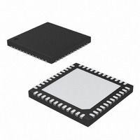
MAX5865ETM+T Maxim Integrated Products, MAX5865ETM+T Datasheet - Page 6

MAX5865ETM+T
Manufacturer Part Number
MAX5865ETM+T
Description
IC ANLG FRONT END 40MSPS 48-TQFN
Manufacturer
Maxim Integrated Products
Datasheet
1.MAX5865ETM.pdf
(26 pages)
Specifications of MAX5865ETM+T
Number Of Bits
10
Number Of Channels
4
Power (watts)
2.10W
Voltage - Supply, Analog
2.7 V ~ 3.3 V
Voltage - Supply, Digital
1.8 V ~ 3.3 V
Package / Case
48-TQFN Exposed Pad
Lead Free Status / RoHS Status
Lead free / RoHS Compliant
Ultra-Low-Power, High-Dynamic-
Performance, 40Msps Analog Front End
ELECTRICAL CHARACTERISTICS (continued)
(V
DAC output amplitude = 0dBFS, differential ADC input, differential DAC output, C
otherwise noted. Typical values are at T
6
Idle Wake-Up Time (with CLK)
Standby Wake-Up Time
Enable Time from Xcvr or Tx to Rx t
Enable Time from Xcvr or Rx to Tx
INTERNAL REFERENCE (REFIN = V
Positive Reference
Negative Reference
Common-Mode Output Voltage
Differential Reference Output
Differential Reference
Temperature Coefficient
Maximum REFP/REFN/COM
Source Current
Maximum REFP/REFN/COM
Sink Current
BUFFERED EXTERNAL REFERENCE (REFIN = 1.024V. V
Reference Input
Differential Reference Output
Common-Mode Output Voltage
Maximum REFP/REFN/COM
Source Current
Maximum REFP/REFN/COM
Sink Current
REFIN Input Resistance
REFIN Input Current
DIGITAL INPUTS (CLK, SCLK, DIN, CS, DD0–DD9)
Input High Threshold
DD
_______________________________________________________________________________________
= 3V, OV
PARAMETER
DD
= 1.8V, internal reference (1.024V), C
t
t
t
ENABLE, Rx
ENABLE, Tx
SYMBOL
WAKE,ST0
WAKE,ST1
DD
I
A
SOURCE
I
REFTC
SOURCE
V
V
V
I
V
V
= +25°C, unless otherwise noted.) (Note 1)
V
I
SINK
. V
COM
REFIN
SINK
REF
COM
DIFF
INH
REFP
, V
From idle to Rx mode with CLK present
during idle, Figure 6, ADC settles to within
1dB SINAD
From idle to Tx mode with CLK present
during idle, Figure 6, DAC settles to 10 LSB
error
From standby to Rx mode, Figure 6, ADC
settles to within 1dB SINAD
From standby to Tx mode, Figure 6, DAC
settles to 10 LSB error
ADC settles to within 1dB SINAD
DAC settles to 10 LSB error
V
V
V
DD0–DD9, CLK, SCLK, DIN, CS
REFN
V
REFP
REFN
REFP
REFP
L
≈ 10pF on all digital outputs, f
and V
- V
- V
- V
- V
COM
REFN
COM
REFP
REFN
COM
, V
CONDITIONS
REFN
are generated internally.)
, and V
COM
REFP
are generated internally.)
CLK
= C
= 40MHz, ADC input amplitude = -0.5dBFS,
REFN
= C
V
0.7 x
OV
+0.49
- 0.15
DD
MIN
COM
DD
/ 2
= 0.33µF, Xcvr mode, unless
V
V
+0.512 +0.534
-0.256
0.256
1.024
0.512
>500
TYP
DD
DD
±30
-0.7
10
10
10
40
10
10
2
2
2
2
/ 2
/ 2
V
+ 0.15
MAX
DD
/ 2
ppm/°C
UNITS
mA
mA
mA
mA
kΩ
µA
µs
µs
µs
µs
V
V
V
V
V
V
V
V


