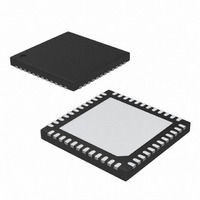
MAX19707ETM+ Maxim Integrated Products, MAX19707ETM+ Datasheet - Page 27

MAX19707ETM+
Manufacturer Part Number
MAX19707ETM+
Description
IC ANLG FRONT END 45MSPS 48-TQFN
Manufacturer
Maxim Integrated Products
Datasheet
1.MAX19707ETM.pdf
(37 pages)
Specifications of MAX19707ETM+
Number Of Bits
10
Number Of Channels
4
Power (watts)
84.6mW
Voltage - Supply, Analog
3V
Voltage - Supply, Digital
3V
Package / Case
48-TQFN Exposed Pad
Lead Free Status / RoHS Status
Lead free / RoHS Compliant
The MAX19707 includes three 12-bit aux-DACs (DAC1,
DAC2, DAC3) with 1µs settling time for controlling VGA,
AGC, and AFC functions. The aux-DAC output range is
0.1V to 2.56V. During power-up, the VGA and AGC out-
puts (DAC2 and DAC3) are at zero. The AFC DAC
(DAC1) is at 1.1V during power-up. The aux-DACs can
be independently controlled through the SPI bus,
except during SHDN mode where the aux-DACs are
turned off completely and the output voltage is set to
zero. In STBY and IDLE modes, the aux-DACs maintain
the last value. On wakeup from SHDN, the aux-DACs
resume the last values.
Loading on the aux-DAC outputs should be carefully
observed to achieve specified settling time and stabili-
ty. The capacitive load must be kept to a maximum of
5pF including package and trace capacitance. The
resistive load must be greater than 200kΩ. If capacitive
loading exceeds 5pF, then add a 10kΩ resistor in
series with the output. Adding the series resistor helps
drive larger load capacitance (< 15pF) at the expense
of slower settling time.
The MAX19707 integrates a 10-bit, 333ksps aux-ADC
with an input 4:1 multiplexer. In the aux-ADC mode reg-
ister, setting bit AD0 begins a conversion with the auxil-
iary ADC. Bit AD0 automatically clears when the
conversion is complete. Setting or clearing AD0 during
a conversion has no effect (see Table 11). Bit AD1
Table 12. Auxiliary ADC Reference
Table 11. Auxiliary ADC Convert
AD1
AD0
0
1
0
1
10-Bit, 333ksps Auxiliary ADC
12-Bit Auxiliary Control DACs
______________________________________________________________________________________
Internal 2.048V Reference (Default)
Internal V
Aux-ADC Start-Convert
Aux-ADC Idle (Default)
SELECTION
SELECTION
DD
10-Bit, 45Msps, Ultra-Low-Power
Reference
determines the internal reference of the auxiliary ADC
(see Table 12). Bits AD2 and AD3 determine the auxil-
iary ADC input source (see Table 13). Bits AD4, AD5,
and AD6 select the number of averages taken when a
single start-convert command is given. The conversion
time increases as the number of averages increases
(see Table 14). The conversion clock can be divided
down from the system clock by properly setting bits
AD7, AD8, and AD9 (see Table 15). The aux-ADC out-
put data can be written out of DOUT by setting bit
AD10 high (see Table 16).
The aux-ADC features a 4:1 input multiplexer to allow
measurements on four input sources. The input sources
are selected by AD3 and AD2 (see Table 13). Two of
the multiplexer inputs (ADC1 and ADC2) can be con-
nected to external sources such as an RF power detec-
tor like the MAX2208 or temperature sensor like the
MAX6613. The other two multiplexer inputs are internal
connections to V
supply voltages. The internal V
tions are made through integrated resistor-dividers that
yield V
aux-ADC voltage reference can be selected between
an internal 2.048V bandgap reference or V
Table 12). The V
allow measurement of an external voltage source with a
full-scale range extending beyond the 2.048V level. The
input source voltage range cannot extend above V
Table 13. Auxiliary ADC Input Source
AD3
0
0
1
1
DD
/ 2 and OV
Analog Front-End
AD2
DD
0
1
0
1
DD
and OV
reference selection is provided to
DD
/ 2 measurement results. The
AUX-ADC INPUT SOURCE
DD
that monitor the power-
DD
ADC1 (Default)
and OV
OV
V
ADC2
DD
DD
/ 2
/ 2
DD
DD
connec-
DD
(see
27
.


