TC500CPE Microchip Technology, TC500CPE Datasheet - Page 7
TC500CPE
Manufacturer Part Number
TC500CPE
Description
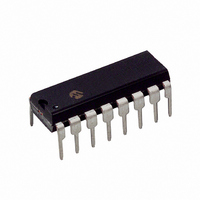
IC ANALOG FRONT END 16BIT 16DIP
Manufacturer
Microchip Technology
Specifications of TC500CPE
Number Of Bits
16
Number Of Channels
1
Power (watts)
10mW
Voltage - Supply, Analog
5V
Voltage - Supply, Digital
4.5 V ~ 7.5 V
Package / Case
16-DIP (0.300", 7.62mm)
Resolution (bits)
17bit
Sampling Rate
10SPS
Input Channel Type
Differential
Data Interface
3-Wire, Serial
Supply Voltage Range - Analog
± 4.5V To ± 7.5V
Supply Current
1mA
Lead Free Status / RoHS Status
Lead free / RoHS Compliant
Other names
158-1021
158-1021
158-1021
Available stocks
Company
Part Number
Manufacturer
Quantity
Price


3.0
The descriptions of the pins are listed in
TABLE 3-1:
© 2008 Microchip Technology Inc.
PDIP, SOIC
CERDIP,
TC500A
TC500,
10
12
13
14
15
16
11
—
—
—
—
—
—
—
—
—
—
—
—
—
1
2
3
4
5
6
7
8
9
PIN DESCRIPTIONS
PDIP, SOIC
Not Used
TC510
PIN FUNCTION TABLE
15
16
18
17
19
23
21
22
24
20
—
—
—
—
—
—
—
—
—
2
3
4
5
6
7
8
9
1
PDIP, SOIC
Not Used
Not Used
Not Used
TC514
22
21
23
27
25
26
28
24
18
13
17
12
16
15
10
20
11
2
3
4
5
6
7
8
9
1
Table
CMPTR OUT Zero crossing comparator output. CMPTR is high during the
Symbol
ACOM
C
DGND
V
C
V
CAP+
V
CH1+
CH2+
CH3+
CH4+
3-1.
CAP-
CH1-
CH2-
CH3-
CH4-
OSC
C
BUF
V
V
V
C
V
REF
REF
REF
REF
OUT
A0
IN
A
B
INT
IN
DD
SS
AZ
+
-
+
+
-
-
-
Integrator output. Integrator capacitor connection.
Negative power supply input (TC500/TC500A only).
Auto-zero input. The auto-zero capacitor connection.
Buffer output. The Integrator capacitor connection.
This pin is grounded in most applications. It is recommended that
ACOM and the input common pin (Ve
Common Mode Range (CMR).
Input. Negative reference capacitor connection.
Input. Positive reference capacitor connection.
Input. External voltage reference (-) connection.
Input. External voltage reference (+) connection.
Negative analog input.
Positive analog input.
Input. Converter phase control MSB. (See input B.)
Input. Converter phase control LSB. The states of A, B place the
TC5XX
when all four phases have been executed:
Phase control input pins: AB =
integration phase when a positive input voltage is being integrated
and is low when a negative input voltage is being integrated. A high-
to-low transition on CMPTR signals the processor that the De-
integrate phase is completed. CMPTR is undefined during the auto-
zero phase. It should be monitored to time the integrator zero phase.
Input. Digital ground.
Input. Power supply positive connection.
Input. Negative power supply converter capacitor (+) connection.
Input. Negative power supply converter capacitor (-) connection.
Output. Negative power supply converter output and reservoir
capacitor connection. This output can be used to power other
devices in the circuit requiring a negative bias voltage.
Oscillator control input. The negative power supply converter
normally runs at a frequency of 100 kHz. The converter oscillator
frequency can be slowed down (to reduce quiescent current) by
connecting an external capacitor between this pin and V
Section 2.0 “Typical Performance Curves”).
Positive analog input pin. MUX channel 1.
Negative analog input pin. MUX channel 1.
Positive analog input pin. MUX channel 2.
Negative analog input pin. MUX channel 2.
Positive analog input pin. MUX channel 3.
Negative analog input pin. MUX channel 3.
Positive analog input pin. MUX channel 4.
Negative analog input pin. MUX channel 4
Multiplexer input channel select input LSB (see A1).
in one of four required phases. A conversion is complete
TC500/A/510/514
Function
00: Integrator zero
01: Auto-zero
10: Integrate
11: De-integrate
n
- or CH
n
-) be within the analog
DS21428E-page 7
DD
(see
Related parts for TC500CPE
Image
Part Number
Description
Manufacturer
Datasheet
Request
R

Part Number:
Description:
(TC500 - TC514) Precision Analog Front Ends
Manufacturer:
Microchip Technology
Datasheet:

Part Number:
Description:
Manufacturer:
Microchip Technology Inc.
Datasheet:
Part Number:
Description:
Manufacturer:
Microchip Technology Inc.
Datasheet:
Part Number:
Description:
Manufacturer:
Microchip Technology Inc.
Datasheet:
Part Number:
Description:
Manufacturer:
Microchip Technology Inc.
Datasheet:
Part Number:
Description:
Manufacturer:
Microchip Technology Inc.
Datasheet:
Part Number:
Description:
Manufacturer:
Microchip Technology Inc.
Datasheet:
Part Number:
Description:
Manufacturer:
Microchip Technology Inc.
Datasheet:
Part Number:
Description:
Manufacturer:
Microchip Technology Inc.
Datasheet: