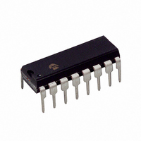
TC500CPE Microchip Technology, TC500CPE Datasheet - Page 11

TC500CPE
Manufacturer Part Number
TC500CPE
Description
IC ANALOG FRONT END 16BIT 16DIP
Manufacturer
Microchip Technology
Specifications of TC500CPE
Number Of Bits
16
Number Of Channels
1
Power (watts)
10mW
Voltage - Supply, Analog
5V
Voltage - Supply, Digital
4.5 V ~ 7.5 V
Package / Case
16-DIP (0.300", 7.62mm)
Resolution (bits)
17bit
Sampling Rate
10SPS
Input Channel Type
Differential
Data Interface
3-Wire, Serial
Supply Voltage Range - Analog
± 4.5V To ± 7.5V
Supply Current
1mA
Lead Free Status / RoHS Status
Lead free / RoHS Compliant
Other names
158-1021
158-1021
158-1021
Available stocks
Company
Part Number
Manufacturer
Quantity
Price
5.0
The TC500/A/510/514 incorporates an auto-zero and
Integrator phase in addition to the input signal Integrate
and reference De-integrate phases. The addition of
these phases reduce system errors, calibration steps
and shorten overrange recovery time. A typical
measurement cycle uses all four phases in the
following order:
1.
2.
3.
4.
TABLE 5-1:
5.1
During this phase, errors due to buffer, integrator and
comparator offset voltages are nulled out by charging
C
voltage.
The external input signal is disconnected from the
internal circuitry by opening the two SW
internal input points connect to analog common. The
reference capacitor is charged to the reference voltage
potential through SW
the integrator and comparator, charges the capacitor
(C
integrator and comparator offset voltages.
5.2
The TC5XX integrates the differential voltage between
the V
be within the device’s Common mode range V
input signal polarity is normally checked via software at
the end of this phase: CMPTR = 1 for positive polarity;
CMPTR = 0 for negative polarity.
© 2008 Microchip Technology Inc.
Conversion Phase
Auto-zero (A = 0, B = 1)
Input Signal Integration (A = 1, B = 0)
Reference Voltage De-integration
(A =1, B = 1)
Integrator Output Zero (A = 0, B = 0)
* Assumes a positive polarity input signal. SW
AZ
AZ
Auto-zero.
Input signal integration.
Reference de-integration.
Integrator output zero.
) with a voltage to compensate for buffer amplifier,
(auto-zero capacitor) with a compensating error
IN
+ and V
TC500/A/510/514 CONVERTER
OPERATION
Auto-zero Phase (AZ)
Analog Input Signal Integration
Phase (INT)
IN
– inputs. The differential voltage must
INTERNAL ANALOG GATE STATUS
R
. A feedback loop, closed around
I
switches. The
CMR
Closed
–
SW
RI
—
—
—
. The
would be closed for a negative input signal.
I
Closed
SW
—
—
—
*
R
+
The internal analog switch status for each of these
phases is summarized in
references the Typical Application.
5.3
The previously charged reference capacitor is
connected with the proper polarity to ramp the
integrator output back to zero. An externally-provided,
precision timer is used to measure the duration of this
phase. The resulting time measurement is proportional
to the magnitude of the applied input voltage.
5.4
This phase ensures the integrator output is at 0V when
the auto-zero phase is entered, and that only system
offset voltages are compensated. This phase is used at
the end of the reference voltage de-integration phase
and MUST be used for ALL TC5XX applications having
resolutions of 12-bits or more. If this phase is not used,
the value of the auto-zero capacitor (C
about 2 to 3 times the value of the integration capacitor
(C
integrator output zero phase should be programmed to
operate until the output of the comparator returns high.
The overall timing system is shown in
INT
SW
) to reduce the effects of charge sharing. The
—
—
—
—
R
Reference Voltage De-integration
Phase (D
Integrator Output Zero Phase (IZ)
-
TC500/A/510/514
Closed
SW
—
—
—
Z
INT
)
Closed
Closed
SW
—
—
R
Table
Closed
Closed
Closed
DS21428E-page 11
SW
5-1. This table
—
Figure
1
AZ
) must be
5-1.
Closed
SW
—
—
—
IZ


