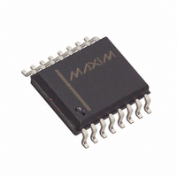
DS1339C-2# Maxim Integrated Products, DS1339C-2# Datasheet - Page 17

DS1339C-2#
Manufacturer Part Number
DS1339C-2#
Description
IC RTC I2C W/ALARM 16-SOIC
Manufacturer
Maxim Integrated Products
Type
Clock/Calendar/Alarmr
Datasheet
1.DS1339U-3.pdf
(20 pages)
Specifications of DS1339C-2#
Time Format
HH:MM:SS (12/24 hr)
Date Format
YY-MM-DD-dd
Interface
I²C, 2-Wire Serial
Voltage - Supply
1.8 V ~ 2.2 V
Operating Temperature
-40°C ~ 85°C
Mounting Type
Surface Mount
Package / Case
16-SOIC (0.300", 7.5mm Width)
Lead Free Status / RoHS Status
Lead free / RoHS Compliant
Memory Size
-
Available stocks
Company
Part Number
Manufacturer
Quantity
Price
Figure 6. Data Transfer on I
Depending upon the state of the R/W bit, two types of data transfer are possible:
The DS1339 can operate in the following two modes:
1) Data transfer from a master transmitter to a slave receiver. The first byte transmitted by the master is
2) Data transfer from a slave transmitter to a master receiver. The first byte (the slave address) is
1) Slave Receiver Mode (Write Mode): Serial data and clock are received through SDA and SCL. After each
Each data transfer is initiated with a START condition and terminated with a STOP condition. The number
of data bytes transferred between START and STOP conditions is not limited, and is determined by the
master device. The information is transferred byte-wise and each receiver acknowledges with a ninth bit.
Acknowledge: Each receiving device, when addressed, is obliged to generate an acknowledge after the
reception of each byte. The master device must generate an extra clock pulse that is associated with this
acknowledge bit.
A device that acknowledges must pull down the SDA line during the acknowledge clock pulse in such a
way that the SDA line is stable LOW during the HIGH period of the acknowledge related clock pulse. Of
course, setup and hold times must be taken into account. A master must signal an end of data to the slave
by not generating an acknowledge bit on the last byte that has been clocked out of the slave. In this case,
the slave must leave the data line HIGH to enable the master to generate the STOP condition.
the slave address. Next follows a number of data bytes. The slave returns an acknowledge bit after each
received byte. Data is transferred with the most significant bit (MSB) first.
transmitted by the master. The slave then returns an acknowledge bit. This is followed by the slave
transmitting a number of data bytes. The master returns an acknowledge bit after all received bytes other
than the last byte. At the end of the last received byte, a “not acknowledge” is returned. The master device
generates all of the serial clock pulses and the START and STOP conditions. A transfer is ended with a
STOP condition or with a repeated START condition. Since a repeated START condition is also the
beginning of the next serial transfer, the bus is not released. Data is transferred with the most significant bit
(MSB) first.
byte is received an acknowledge bit is transmitted. START and STOP conditions are recognized as the
beginning and end of a serial transfer. Address recognition is performed by hardware after reception of the
slave address and direction bit
START condition is generated by the master. The slave address byte contains the 7-bit DS1339 address,
which is 1101000, followed by the direction bit (R/W), which is 0 for a write. After receiving and decoding
the slave address byte the slave outputs an acknowledge on the SDA line. After the DS1339
acknowledges the slave address + write bit, the master transmits a register address to the DS1339. This
2
C Serial Bus
(Figure
7). The slave address byte is the first byte received after the
17 of 20
DS1339 I
2
C Serial Real-Time Clock


