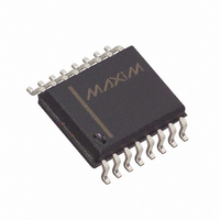
DS1339C-2# Maxim Integrated Products, DS1339C-2# Datasheet - Page 14

DS1339C-2#
Manufacturer Part Number
DS1339C-2#
Description
IC RTC I2C W/ALARM 16-SOIC
Manufacturer
Maxim Integrated Products
Type
Clock/Calendar/Alarmr
Datasheet
1.DS1339U-3.pdf
(20 pages)
Specifications of DS1339C-2#
Time Format
HH:MM:SS (12/24 hr)
Date Format
YY-MM-DD-dd
Interface
I²C, 2-Wire Serial
Voltage - Supply
1.8 V ~ 2.2 V
Operating Temperature
-40°C ~ 85°C
Mounting Type
Surface Mount
Package / Case
16-SOIC (0.300", 7.5mm Width)
Lead Free Status / RoHS Status
Lead free / RoHS Compliant
Memory Size
-
Available stocks
Company
Part Number
Manufacturer
Quantity
Price
2
DS1339 I
C Serial Real-Time Clock
Bit 2: Interrupt Control (INTCN). This bit controls the relationship between the two alarms and the interrupt output
pins. When the INTCN bit is set to logic 1, a match between the timekeeping registers and the alarm 1 or alarm 2
registers activate the SQW/INT pin (provided that the alarm is enabled). When the INTCN bit is set to logic 0, a
square wave is output on the SQW/INT pin. This bit is set to logic 0 when power is first applied.
Bit 1: Alarm 2 Interrupt Enable (A2IE). When set to a logic 1, this bit permits the Alarm 2 Flag (A2F) bit in the
status register to assert SQW/INT (when INTCN = 1). When the A2IE bit is set to logic 0 or INTCN is set to logic 0,
the A2F bit does not initiate an interrupt signal. The A2IE bit is disabled (logic 0) when power is first applied.
Bit 0: Alarm 1 Interrupt Enable (A1IE). When set to logic 1, this bit permits the Alarm 1 Flag (A1F) bit in the
status register to assert SQW/INT (when INTCN = 1). When the A1IE bit is set to logic 0 or INTCN is set to logic 0,
the A1F bit does not initiate an interrupt signal. The A1IE bit is disabled (logic 0) when power is first applied.
STATUS REGISTER (0Fh)
BIT 7
BIT 6
BIT 5
BIT 4
BIT 3
BIT 2
BIT 1
BIT 0
OSF
0
0
0
0
0
A2F
A1F
Bit 7: Oscillator Stop Flag (OSF). A logic 1 in this bit indicates that the oscillator either is stopped or was stopped
for some period of time and may be used to judge the validity of the clock and date data. This bit is edge triggered
and is set to logic 1 when the oscillator stops. The following are examples of conditions that can cause the OSF bit
to be set:
1) The first time power is applied.
2) The voltage on both V
and V
are insufficient to support oscillation.
CC
BACKUP
3) The EOSC bit is turned off.
4) External influences on the crystal (e.g., noise, leakage, etc.).
This bit remains at logic 1 until written to logic 0. This bit can only be written to a logic 0.
Bit 1: Alarm 2 Flag (A2F). A logic 1 in the Alarm 2 Flag bit indicates that the time matched the alarm 2 registers. If
the A2IE bit is a logic 1 and the INTCN bit is set to a logic 1, the SQW/INT pin is also asserted. A2F is cleared
when written to logic 0. This bit can only be written to logic 0. Attempting to write to logic 1 leaves the value
unchanged.
Bit 0: Alarm 1 Flag (A1F). A logic 1 in the Alarm 1 Flag bit indicates that the time matched the alarm 1 registers. If
the A1IE bit is a logic 1 and the INTCN bit is set to a logic 1, the SQW/INT pin is also asserted. A1F is cleared
when written to logic 0. This bit can only be written to logic 0. Attempting to write to logic 1 leaves the value
unchanged.
14 of 20


