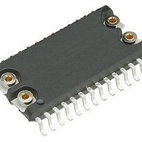
M48T201Y-70MH1E STMicroelectronics, M48T201Y-70MH1E Datasheet - Page 11

M48T201Y-70MH1E
Manufacturer Part Number
M48T201Y-70MH1E
Description
IC SUPERVISOR TIMEKPR 5V 44-SOH
Manufacturer
STMicroelectronics
Series
Timekeeper®r
Type
Clock/Calendar/NVSRAMr
Datasheet
1.M48T201V-85MH1F.pdf
(37 pages)
Specifications of M48T201Y-70MH1E
Memory Size
External
Time Format
HH:MM:SS (24 hr)
Date Format
YY-MM-DD-dd
Interface
Parallel
Voltage - Supply
4.5 V ~ 5.5 V
Operating Temperature
0°C ~ 70°C
Mounting Type
Surface Mount
Package / Case
44-SOH
Number Of Voltages Monitored
1
Monitored Voltage
3.3 V, 5 V
Manual Reset
Not Resettable
Watchdog
Watchdog
Battery Backup Switching
Backup
Supply Voltage (max)
5.5 V
Supply Voltage (min)
4.5 V
Supply Current (typ)
15000 uA
Maximum Power Dissipation
1000 mW
Maximum Operating Temperature
+ 70 C
Mounting Style
SMD/SMT
Minimum Operating Temperature
0 C
Power Fail Detection
Yes
Lead Free Status / RoHS Status
Contains lead / RoHS non-compliant
Other names
497-2840-5
M48T201Y-70MH1
M48T201Y-70MH1
M48T201Y, M48T201V
Note:
2.2
Figure 4.
ADDRESS
G
G CON
E
Table 2.
1. See
X = V
Read mode
The M48T201Y/V executes a READ cycle whenever W (WRITE enable) is high and E (chip
enable) is low. The unique address specified by the address inputs (A0-A18) defines which
one of the on-chip TIMEKEEPER
When the address presented to the M48T201Y/V is in the range of 7FFFFh-7FFF0h, one of
the on-board TIMEKEEPER registers is accessed and valid data will be available to the
eight data output drivers within t
the E and G access times are also satisfied. If they are not, then data access must be
measured from the latter occurring signal (E or G) and the limiting parameter is either t
for E or t
TIMEKEEPER registers is selected for READ, the G
throughout the READ cycle.
When the address value presented to the M48T201Y/V is outside the range of
TIMEKEEPER registers, an external SRAM location will be selected. In this case the G
signal will be passed to the G
G
CON
Deselect
Deselect
Deselect
WRITE
READ
READ
Mode
IH
timing when switching between RTC and external SRAM
Table 14 on page 30
7FFF0h - 7FFFFh
or V
GLQV
RTC
IL
Operating modes
; V
for G rather than the address access time. When one of the on-chip
V
SO
SO
4.5 V to 5.5 V
3.0 V to 3.6 V
to V
= battery backup switchover voltage
V
V
PFD
or
SO
CC
External SRAM
00000h - 7FFEFh
for details.
(1)
(min)
tAOEL
CON
(1)
AVQV
®
pin, with the specified delay times of t
registers or external SRAM locations is to be accessed.
after the address input signal is stable, providing that
V
V
V
V
E
X
X
IH
IL
IL
IL
7FFF0h - 7FFFFh
tAOEH
RTC
V
V
G
X
X
X
X
IH
IL
CON
tOERL
signal will remain inactive
V
V
V
W
X
X
X
IH
IH
IL
00000h - 7FFEFh
External SRAM
High-Z
High-Z
High-Z
High-Z
DQ7-
D
DQ0
D
OUT
IN
AOEL
CMOS standby
Battery backup
AI02333
tRO
or t
Standby
Power
Active
Active
Active
OERL
Operation
.
ELQV
11/37


