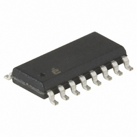
CDP68HC68T1M2 Intersil, CDP68HC68T1M2 Datasheet - Page 9

CDP68HC68T1M2
Manufacturer Part Number
CDP68HC68T1M2
Description
IC RTC 32X8 NVSRAM CMOS 16-SOIC
Manufacturer
Intersil
Type
Clock/Calendar/NVSRAMr
Datasheet
1.CDP68HC68T1EZ.pdf
(23 pages)
Specifications of CDP68HC68T1M2
Memory Size
32B
Time Format
HH:MM:SS (12/24 hr)
Date Format
YY-MM-DD-dd
Interface
SPI, 3-Wire Serial
Voltage - Supply
3 V ~ 6 V
Operating Temperature
-40°C ~ 85°C
Mounting Type
Surface Mount
Package / Case
16-SOIC (0.300", 7.5mm Width)
Digital Ic Case Style
SOIC
No. Of Pins
16
Operating Temperature Range
-40°C To +85°C
Peak Reflow Compatible (260 C)
No
Current Rating
12A
Leaded Process Compatible
No
Rohs Compliant
No
Bus Type
Serial (3-Wire, SPI)
Operating Supply Voltage (typ)
3.3/5V
Package Type
SOIC W
Operating Supply Voltage (max)
6V
Operating Supply Voltage (min)
3V
Operating Temperature Classification
Industrial
Operating Temperature (max)
85C
Operating Temperature (min)
-40C
Pin Count
16
Mounting
Surface Mount
Lead Free Status / RoHS Status
Contains lead / RoHS non-compliant
Available stocks
Company
Part Number
Manufacturer
Quantity
Price
Company:
Part Number:
CDP68HC68T1M2Z
Manufacturer:
Intersil
Quantity:
1 716
Part Number:
CDP68HC68T1M2Z
Manufacturer:
INTERSIL
Quantity:
20 000
Power Sensing
When Power Sensing is enabled (Bit 5 = 1 in Interrupt
Control Register), AC transitions are sensed at the LINE input
pin. Threshold detectors determine when transitions cease.
After a delay of 2.68ms to 4.64ms, plus the external input
circuit RC time constant, an interrupt is generated and a bit is
set in the Status Register. This bit can then be sampled to see
if system power has turned back on. See "Functional
Description", Line pin on page 10. The power-sense circuitry
operates by sensing the level of the voltage presented at the
line input pin. This voltage is centered around V
long as it is either plus or minus a threshold (about 1V) from
V
signal present, remaining in this V
minimum of 2.68ms will activate the power-sense circuit. The
larger the amplitude of the AC signal, the less time it spends
in the V
detected. A 60Hz, 10V
DD
a power-sense failure will not be indicated. With an AC
DD
FROM SYSTEM
POWER
FIGURE 4. POWER-DOWN FUNCTIONAL DIAGRAM
window, and the less likely a power failure will be
V
INTERRUPT
CONTROL
REGISTER
REAL-TIME CLOCK
CDP68HC68T1
SYS
INTERFACE
I
SERIAL
V
DD
0V
(See Figure 3)
P-P
sinewave voltage is an applicable
CPUR
OUT
CLK
PSE
9
DD
TO SYSTEM
POWER CONTROL
window longer than a
MISO
MOSI
FIGURE 3. POWER-SENSING FUNCTIONAL DIAGRAM
OSC
RESET
V
CDP68HC05C4B
DD
DD
CPU
and as
XTAL IN
XTAL OUT
LINE
REAL-TIME CLOCK
STATUS REGISTER
CDP68HC68T1
CDP68HC68T1
I
INT
FIGURE 5. POWER-UP FUNCTIONAL DIAGRAM (INITIATED
signal to present at the LINE input pin to setup the power
sense function.
Power-Down
Power-down is a processor-directed operation. A bit is set in
the Interrupt Control Register to initiate operation. Three pins
are affected. The PSE (Power Supply Enable) output,
normally high, is placed low. The CLK OUT is placed low.
The CPUR output, connected to the processors reset input
is also placed low. In addition, the Serial Interface is
disabled.
Power-Up
Two conditions will terminate the Power-Down mode.
1. The first condition (see Figure 5) requires an interrupt.
The interrupt can be generated by the alarm circuit, the
programmable periodic interrupt signal, or the power
sense circuit.
REAL-TIME CLOCK
CDP68HC68T1
INTERRUPT
INTERFACE
BY INTERRUPT SIGNAL
POWER-UP
PERIODIC
CIRCUIT
INT
POWER
SIGNAL
ALARM
SERIAL
SENSE
(See Figures 5 and 6)
CDP68HC05C16B
OR
(See Figure 4)
CPU
CPUR
CLK
OUT
PSE
INT
MISO
MOSI
October 29, 2007
FN1547.8


