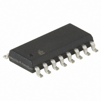
CDP68HC68T1M2 Intersil, CDP68HC68T1M2 Datasheet - Page 14

CDP68HC68T1M2
Manufacturer Part Number
CDP68HC68T1M2
Description
IC RTC 32X8 NVSRAM CMOS 16-SOIC
Manufacturer
Intersil
Type
Clock/Calendar/NVSRAMr
Datasheet
1.CDP68HC68T1EZ.pdf
(23 pages)
Specifications of CDP68HC68T1M2
Memory Size
32B
Time Format
HH:MM:SS (12/24 hr)
Date Format
YY-MM-DD-dd
Interface
SPI, 3-Wire Serial
Voltage - Supply
3 V ~ 6 V
Operating Temperature
-40°C ~ 85°C
Mounting Type
Surface Mount
Package / Case
16-SOIC (0.300", 7.5mm Width)
Digital Ic Case Style
SOIC
No. Of Pins
16
Operating Temperature Range
-40°C To +85°C
Peak Reflow Compatible (260 C)
No
Current Rating
12A
Leaded Process Compatible
No
Rohs Compliant
No
Bus Type
Serial (3-Wire, SPI)
Operating Supply Voltage (typ)
3.3/5V
Package Type
SOIC W
Operating Supply Voltage (max)
6V
Operating Supply Voltage (min)
3V
Operating Temperature Classification
Industrial
Operating Temperature (max)
85C
Operating Temperature (min)
-40C
Pin Count
16
Mounting
Surface Mount
Lead Free Status / RoHS Status
Contains lead / RoHS non-compliant
Available stocks
Company
Part Number
Manufacturer
Quantity
Price
Company:
Part Number:
CDP68HC68T1M2Z
Manufacturer:
Intersil
Quantity:
1 716
Part Number:
CDP68HC68T1M2Z
Manufacturer:
INTERSIL
Quantity:
20 000
Functional Description
The Serial Peripheral Interface (SPI) utilized by the
CDP68HC68T1 is a serial synchronous bus for address and
data transfers. The clock, which is generated by the
microcomputer is active only during address and data
transfers. In systems using the CDP68HC05C4 or
CDP68HC05D2, the inactive clock polarity is determined by
the CPOL bit in the microcomputer’s Control Register. A
unique feature of the CDP68HC68T1 is that it automatically
determines the level of the inactive clock by sampling SCK
when CE becomes active (see Figure 8). Input data (MOSI)
is latched internally on the internal strobe edge and output
data (MISO) is shifted out on the shift edge, as defined by
Figure 8. There is one clock for each data bit transferred
(address, as well as data bits are transferred in groups of 8).
NOTE: “CPOL” is a bit that is set in the microcomputer’s Control
Register.
NOTE: SCK can be either polarity.
CPOL = 0
CPOL = 1
FIGURE 8. SERIAL RAM CLOCK (SCK) AS A FUNCTION OF
04
5
6
7
BIT
SCK (NOTE)
W/R
CE
SCK
CE
SCK
MOSI
7
MCU CLOCK POLARITY (CPOL)
MOSI
CE
A0 through A4
CLK RAM
0
W/R
6
0
14
FIGURE 9. ADDRESS/CONTROL BYTE-TRANSFER WAVEFORMS
SHIFT
SHIFT
W/R
CLK RAM
MSB
5
INTERNAL
INTERNAL
STROBE
STROBE
0
MSB -1
Selects 5-bit HEX Address of RAM or specifies Clock Register. Most Significant Address
Bit. If equal to “1”, A0 through A4 selects a Clock Register. If equal to “0”, A0 through A4
selects one of 32 RAM locations. Must be set to ”0” when not in Test Mode 7W/R W/R = “1”
initiates one or more WRITE cycles.W/R = “0”, initiates one or more READ cycles.
CLOCK
RAM
CDP68HC68T1
A4
A4
4
A3
Address and Data Format
There are three types of serial transfer:
The Address/Control and Data bytes are shifted MSB first,
Into the serial data input (MOSI) and out of the serial data
output (MISO).
Any transfer of data requires an Address/Control byte to
specify a Write or Read operation and to select a Clock or
RAM location, followed by one or more bytes of data.
Data is transferred out of MISO for a Read and into MOSI for
a Write operation.
Address/Control Byte - (
It is always the first byte received after CE goes true. To
transmit a new address, CE must first go false and then true
again. Bit 5 is used to select between Clock and RAM
locations.
1. Address Control - Figure 9.
2. READ or WRITE Data - Figure 10.
3. Watchdog Reset (actually a non-transfer) Figure 11.
A2
A3
3
A1
A0
A2
2
see Figure 9)
A1
1
October 29, 2007
A0
0
FN1547.8


