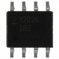
ISL12026IBZ Intersil, ISL12026IBZ Datasheet - Page 12

ISL12026IBZ
Manufacturer Part Number
ISL12026IBZ
Description
IC RTC/CALENDAR EEPROM 8-SOIC
Manufacturer
Intersil
Type
Clock/Calendar/EEPROMr
Specifications of ISL12026IBZ
Memory Size
4K (512 x 8)
Time Format
HH:MM:SS (12/24 hr)
Date Format
YY-MM-DD-dd
Interface
I²C, 2-Wire Serial
Voltage - Supply
2.7 V ~ 5.5 V
Operating Temperature
-40°C ~ 85°C
Mounting Type
Surface Mount
Package / Case
8-SOIC (3.9mm Width)
Clock Format
HH
Clock Ic Type
RTC
Interface Type
I2C, Serial
Memory Configuration
512 X 8
Supply Voltage Range
2.7V To 5.5V
Digital Ic Case Style
SOIC
Rohs Compliant
Yes
Lead Free Status / RoHS Status
Lead free / RoHS Compliant
Available stocks
Company
Part Number
Manufacturer
Quantity
Price
Company:
Part Number:
ISL12026IBZ
Manufacturer:
INTELSEL
Quantity:
60
Part Number:
ISL12026IBZ
Manufacturer:
INTERSIL
Quantity:
20 000
Part Number:
ISL12026IBZ-T
Manufacturer:
INTERSIL
Quantity:
20 000
DTR Register - DTR2, DTR1, DTR0: Digital
Trimming Register
The digital trimming Bits DTR2, DTR1 and DTR0 adjust the
number of counts per second and average the ppm error to
achieve better accuracy.
DTR2 is a sign bit. DTR2 = 0 means frequency
compensation is > 0. DTR2 = 1 means frequency
compensation is < 0.
DTR1 and DTR0 are scale bits. DTR1 gives 10 ppm
adjustment and DTR0 gives 20 ppm adjustment.
A range from -30ppm to +30ppm can be represented by
using three bits above.
PWR Register: SBIB, BSW
SBIB: - Serial Bus Interface (Enable)
The serial bus can be disabled in battery backup mode by
setting this bit to “1”. This will minimize power drain on the
battery. The Serial Interface can be enabled in battery
backup mode by setting this bit to “0”. (default is “0”). See
Reset and Power Control section.
BSW: Power Control Bit
The Power Control bit, BSW, determines the conditions for
switching between V
options.
Option 1. Standard/Default Mode: Set “BSW = 0”
Option 2. Legacy Mode: Set “BSW = 1”
See Power Control Operation later in this document for more
details. Also see “I
backup and LVR Operation” in the Applications section for
important details.
Device Operation
Writing to the Clock/Control Registers
Changing any of the bits of the clock/control registers
requires the following steps:
DTR2
0
0
0
0
1
1
1
1
DTR REGISTER
TABLE 5. DIGITAL TRIMMING REGISTERS
DTR1
0
1
0
1
0
1
0
1
2
C Communications During Battery
DD
and Back Up Battery. There are two
DTR0
0
0
1
1
0
0
1
1
12
ESTIMATED FREQUENCY
PPM
+10
+20
+30
-10
-20
-30
0
0
ISL12026
Write all eight bytes to the RTC registers, or one byte to the
SR, or one to five bytes to the control registers. This
sequence starts with a start bit, requires a slave byte of
“11011110” and an address within the CCR and is terminated
by a stop bit. A write to the EEPROM registers in the CCR
will initiate a non-volatile write cycle and will take up to 20ms
to complete. A write to the RTC registers (SRAM) will require
much shorter cycle time (t = t
have no effect. The RWEL bit is reset by the completion of a
write to the CCR, so the sequence must be repeated to
again initiate another change to the CCR contents. If the
sequence is not completed for any reason (by sending an
incorrect number of bits or sending a start instead of a stop,
for example) the RWEL bit is not reset and the device
remains in an active mode. Writing all zeros to the status
register resets both the WEL and RWEL bits. A read
operation occurring between any of the previous operations
will not interrupt the register write operation.
Alarm Operation
Since the alarm works as a comparison between the alarm
registers and the RTC registers, it is ideal for notifying a host
processor of a particular time event and trigger some action
as a result. The host can be notified by either a hardware
interrupt (the IRQ/F
(SR) Alarm bits. These two volatile bits (AL1for Alarm 1 and
AL0 for Alarm 0), indicate if an alarm has happened. The bits
are set on an alarm condition regardless of whether the IRQ/
F
register are reset by the falling edge of the eighth clock of
status register read.
There are two alarm operation modes: Single Event and
periodic Interrupt Mode:
1. Write a 02h to the Status Register to set the Write Enable
2. Write a 06h to the Status Register to set both the Register
1. Single Event Mode is enabled by setting the AL0E or
2. Interrupt Mode (or “Pulsed Interrupt Mode” or PIM) is
OUT
Latch (WEL). This is a volatile operation, so there is no
delay after the write. (Operation preceded by a start and
ended with a stop).
Write Enable Latch (RWEL) and the WEL bit. This is also
a volatile cycle. The zeros in the data byte are required.
(Operation proceeded by a start and ended with a stop).
AL1E bit to “1”, the IM bit to “0”, and disabling the
frequency output. This mode permits a one-time match
between the alarm registers and the RTC registers. Once
this match occurs, the AL0 or AL1 bit is set to “1” and the
IRQ/F
until the AL0 or AL1 bit is read, which will automatically
resets it. Both Alarm registers can be set at the same time
to trigger alarms. The IRQ/F
either alarm, and will need to be cleared to enable
triggering by a subsequent alarm. Polling the SR will
reveal which alarm has been set.
enabled by setting the AL0E or AL1E bit to “1” the IM bit
to “1”, and disabling the frequency output. If both AL0E
interrupt is enabled. The AL1 and AL0 bits in the status
OUT
output will be pulled low and will remain low
OUT
pin) or by polling the Status Register
BUF
OUT
). Writes to undefined areas
output will be set by
October 23, 2006
FN8231.5


