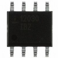
ISL12030IBZ-T Intersil, ISL12030IBZ-T Datasheet - Page 15

ISL12030IBZ-T
Manufacturer Part Number
ISL12030IBZ-T
Description
IC RTC/CALENDAR EEPROM 8-SOIC
Manufacturer
Intersil
Type
Clock/Calendar/NVSRAMr
Datasheet
1.ISL12030IBZ-T.pdf
(17 pages)
Specifications of ISL12030IBZ-T
Memory Size
1K (128 x 8)
Time Format
HH:MM:SS:hh (12/24 hr)
Date Format
YY-MM-DD-dd
Interface
I²C, 2-Wire Serial
Voltage - Supply
2.7 V ~ 5.5 V
Operating Temperature
-40°C ~ 85°C
Mounting Type
Surface Mount
Package / Case
8-SOIC (3.9mm Width)
Rohs Compliant
Yes
Lead Free Status / RoHS Status
Lead free / RoHS Compliant
Other names
ISL12030IBZ-TTR
Available stocks
Company
Part Number
Manufacturer
Quantity
Price
Company:
Part Number:
ISL12030IBZ-T
Manufacturer:
Intersil
Quantity:
2 500
Application Section
AC Input Circuits
The AC input ideally will have a 2.5V
input, so this is the target for any signal conditioning circuitry
for the 50/60Hz waveform. Note that the peak-to-peak
amplitude can range from 1V
best to keep the max signal level just below V
input provides DC offset so AC coupling with a series
capacitor is advised.
If the AC power supply has a transformer, the secondary
output can be used for clocking with a resistor divider and
series AC coupling capacitor. A sample circuit is shown in
Figure 8. Values for R
peak-to-peak range on the secondary voltage in order to
match the input of the ISL12030. C
up to 300Hz or so, and in most cases, 0.47µF should be the
selected value for a ±20% tolerance device.
120VAC
50/60Hz
120VAC
50/60Hz
1
/R
2
are chosen depending on the
15
P-P
up to V
IN
FIGURE 8. AC INPUT USING A TRANSFORMER SECONDARY
FIGURE 9. USING THE V
P-P
can be sized to pass
DD
sine wave at the
, although it is
DD
. The AC
R1
R1
ISL12030
DD
R2
C1
SUPPLY TO GATE THE AC INPUT
R2
The AC input to the ISL12030 can be damaged if subjected
to a normal AC waveform when V
can happen in circuits where there is a local LDO or power
switch for placing circuitry in standby, while the AC main is
still switched ON. Figure 8 shows a modified version of the
Figure 9 circuit, which uses an emitter follower to essentially
turn off the AC input waveform if the V
Adding a Super Capacitor Backup
Since any loss of V
including control and RTC register sections, then having
some form of V
connections for a super capacitor backup using V
normal source and a signal diode for charging. Be careful
not to use a normal Schottky diode as the leakage will
greatly reduce the backup life of the super capacitor.
This form of backup should yield at least one full day of
backup time, assuming the SCL/SDA pins and their pull-ups
are pulled to ground on powerdown.
CIN
VDD
VIN (AC) = 1.5V
CIN
DD
ISL12030
backup is a good idea. Figure 10 shows
DD
P-P
power will reset the SRAM memory
TO 5V
VIN (AC) = 1.5V
ISL12030
P-P
DD
P-P
is powered down. This
DD
TO VDD (MAX)
supply goes down.
January 15, 2008
DD
for the
FN6617.1


