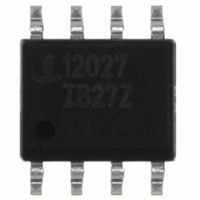
ISL12027IB27Z-T Intersil, ISL12027IB27Z-T Datasheet - Page 20

ISL12027IB27Z-T
Manufacturer Part Number
ISL12027IB27Z-T
Description
IC RTC/CALENDAR EEPROM 8-SOIC
Manufacturer
Intersil
Type
Clock/Calendar/Supervisor/EEPROMr
Datasheet
1.ISL12027IB27Z-T.pdf
(28 pages)
Specifications of ISL12027IB27Z-T
Memory Size
4K (512 x 8)
Time Format
HH:MM:SS (12/24 hr)
Date Format
YY-MM-DD-dd
Interface
I²C, 2-Wire Serial
Voltage - Supply
2.7 V ~ 5.5 V
Operating Temperature
-40°C ~ 85°C
Mounting Type
Surface Mount
Package / Case
8-SOIC (3.9mm Width)
Bus Type
Serial (I2C)
Operating Supply Voltage (typ)
3.3V
Operating Supply Voltage (max)
5.5V
Operating Supply Voltage (min)
2.7V
Operating Temperature Classification
Industrial
Operating Temperature (max)
85C
Operating Temperature (min)
-40C
Pin Count
8
Mounting
Surface Mount
Rohs Compliant
YES
Lead Free Status / RoHS Status
Lead free / RoHS Compliant
Other names
ISL12027IB27Z-TTR
Available stocks
Company
Part Number
Manufacturer
Quantity
Price
Company:
Part Number:
ISL12027IB27Z-T
Manufacturer:
Intersil
Quantity:
390
Acknowledge Polling
Disabling of the inputs during non-volatile write cycles can
be used to take advantage of the typical 5ms write cycle
time. Once the stop condition is issued to indicate the end of
the master’s byte load operation, the ISL12027 initiates the
internal non-volatile write cycle. Acknowledge polling can
begin immediately. To do this, the master issues a start
condition followed by the Memory Array Slave Address Byte
for a write or read operation (AEh or AFh). If the ISL12027 is
still busy with the non-volatile write cycle, then no ACK will
be returned. When the ISL12027 has completed the write
operation, an ACK is returned and the host can proceed with
the read or write operation. Refer to the flow chart in
Figure 24. Note: Do not use the CCR Slave byte (DEh or
DFh) for Acknowledge Polling.
Read Operations
There are three basic read operations: Current Address
Read, Random Read and Sequential Read.
SIGNALS FROM
SIGNALS FROM
THE MASTER
SDA BUS
THE SLAVE
ADDRESS POINTER ENDS
6 BYTES
FIGURE 21. WRITING 12 BYTES TO A 16-BYTE MEMORY PAGE STARTING AT ADDRESS 10
SIGNALS FROM
SIGNALS FROM
ADDRESS = 5
AT ADDR = 5
THE MASTER
SDA BUS
THE SLAVE
A
R
S
T
T
20
1
ADDRESS
SLAVE
1
1
1
S
A
R
T
T
0
1
A
C
K
ADDRESS
FIGURE 20. BYTE WRITE SEQUENCE
FIGURE 22. PAGE WRITE SEQUENCE
0 0 0 0 0 0 0
SLAVE
ISL12027, ISL12027A
ADDRESS 1
1
WORD
1
1
0
A
C
K
0 0 0 0 0 0 0
ADDRESS 1
WORD
A
C
K
ADDRESS 0
Current Address Read
Internally the ISL12027 contains an address counter that
maintains the address of the last word read incremented by
one. Therefore, if the last read was to address n, the next
read operation would access data from address n + 1. On
power-up, the 16 bit address is initialized to 0h. In this way, a
current address read immediately after the power on reset
can download the entire contents of memory starting at the
first location. Upon receipt of the Slave Address Byte with
the R/W bit set to one, the ISL12027 issues an
acknowledge, then transmits 8 data bits. The master
terminates the read operation by not responding with an
acknowledge during the ninth clock and issuing a stop
condition. Refer to Figure 23 for the address, acknowledge,
and data transfer sequence.
It should be noted that the ninth clock cycle of the read
operation is not a “don’t care.” To terminate a read operation,
the master must either issue a stop condition during the
ninth cycle or hold SDA HIGH during the ninth clock cycle
and then issue a stop condition.
WORD
ADDRESS
A
C
K
10
ADDRESS 0
WORD
A
C
K
1 ≤ n ≤ 16 FOR EEPROM ARRAY
1 ≤ n ≤ 8 FOR CCR
DATA
A
C
K
(1)
6 BYTES
DATA
ADDRESS
A
C
K
15
O
S
T
P
DATA
(n)
A
C
K
S
O
P
August 12, 2010
T
FN8232.8


