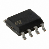
M41T82RM6F STMicroelectronics, M41T82RM6F Datasheet - Page 17

M41T82RM6F
Manufacturer Part Number
M41T82RM6F
Description
IC RTC SERIAL W/BATT SW 8-SOIC
Manufacturer
STMicroelectronics
Type
Clock/Calendar/Alarmr
Datasheet
1.M41T82SM6F.pdf
(61 pages)
Specifications of M41T82RM6F
Memory Size
32B
Time Format
HH:MM:SS:hh (24 hr)
Date Format
YY-MM-DD-dd
Interface
I²C, 2-Wire Serial
Voltage - Supply
2.7 V ~ 5.5 V
Operating Temperature
-40°C ~ 85°C
Mounting Type
Surface Mount
Package / Case
8-SOIC (3.9mm Width)
Lead Free Status / RoHS Status
Lead free / RoHS Compliant
Other names
497-8279-2
M41T82RM6F
M41T82RM6F
Available stocks
Company
Part Number
Manufacturer
Quantity
Price
Company:
Part Number:
M41T82RM6F
Manufacturer:
ST
Quantity:
15 734
M41T82-M41T83
2.3
Figure 15. Write mode sequence
BUS ACTIVITY:
MASTER
SDA LINE
BUS ACTIVITY:
Write mode
In this mode the master transmitter transmits to the M41T8x slave receiver. Bus protocol is
shown in
placed on the bus and indicates to the addressed device that word address “An” will follow
and is to be written to the on-chip address pointer. The data word to be written to the
memory is strobed in next and the internal address pointer is incremented to the next
address location on the reception of an acknowledge clock. The M41T8x slave receiver will
send an acknowledge clock to the master transmitter after it has received the slave address
see
byte.
As in the case of reading, some registers and memory locations are written directly, but the
RTC counters are written via a set of eight buffer/transfer registers at addresses 00h to 07h.
The user will write the date and time information sequentially, and then, at the end of the I
write cycle or when the address pointer increments beyond 07h, the buffer/transfer registers
will be copied into the RTC counters. All the time parameters - fractions, seconds, minutes,
hours, day, date, month, year, and century bits - are copied simultaneously.
Whatever value is in the buffer/transfer registers will be copied to the counters, so if the user
only changes one of the eight bytes, the remaining seven bytes will receive the unchanged
contents of the buffer/transfer registers, which will contain whatever was in the counters at
the start of the write access.
For example, if the user starts a write cycle on Monday, November 16, 2009, at 17:52:27.03,
and writes a 22 to the minutes registers, the value Monday, November 16, 2009,
17:52:22.03 will be written back into the counters. At the start of the write cycle, the eight
bytes of counters were copied into the buffer/transfer registers. Then, the seconds register
was overwritten. Finally, the eight bytes were copied back into the counters with the result
that the seconds value was changed.
Figure 12 on page 15
S
ADDRESS
Figure 15.
SLAVE
Following the START condition and slave address, a logic 0 (R/W = 0) is
ADDRESS (An)
WORD
and again after it has received the word address and each data
Doc ID 12578 Rev 12
DATA n
DATA n+1
DATA n+X
Operation
P
AI00591
17/61
2
C


