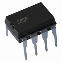
PCF8583P/F5,112 NXP Semiconductors, PCF8583P/F5,112 Datasheet - Page 29

PCF8583P/F5,112
Manufacturer Part Number
PCF8583P/F5,112
Description
IC CLK/CALENDAR 240X8 RAM 8-DIP
Manufacturer
NXP Semiconductors
Type
Clock/Calendar/NVSRAMr
Datasheet
1.PCF8583T5518.pdf
(37 pages)
Specifications of PCF8583P/F5,112
Package / Case
8-DIP (0.300", 7.62mm)
Memory Size
240B
Time Format
HH:MM:SS (12/24 hr)
Date Format
YY-MM-DD
Interface
I²C, 2-Wire Serial
Voltage - Supply
1 V ~ 6 V
Operating Temperature
-40°C ~ 85°C
Mounting Type
Through Hole
Mounting Style
Through Hole
Lead Free Status / RoHS Status
Lead free / RoHS Compliant
Lead Free Status / RoHS Status
Lead free / RoHS Compliant, Lead free / RoHS Compliant
Other names
568-1084-5
935261345112
PCF8583PN
935261345112
PCF8583PN
Available stocks
Company
Part Number
Manufacturer
Quantity
Price
Company:
Part Number:
PCF8583P/F5,112
Manufacturer:
LTC
Quantity:
147
NXP Semiconductors
13. Soldering of SMD packages
PCF8583
Product data sheet
13.1 Introduction to soldering
13.2 Wave and reflow soldering
13.3 Wave soldering
This text provides a very brief insight into a complex technology. A more in-depth account
of soldering ICs can be found in Application Note AN10365 “Surface mount reflow
soldering description”.
Soldering is one of the most common methods through which packages are attached to
Printed Circuit Boards (PCBs), to form electrical circuits. The soldered joint provides both
the mechanical and the electrical connection. There is no single soldering method that is
ideal for all IC packages. Wave soldering is often preferred when through-hole and
Surface Mount Devices (SMDs) are mixed on one printed wiring board; however, it is not
suitable for fine pitch SMDs. Reflow soldering is ideal for the small pitches and high
densities that come with increased miniaturization.
Wave soldering is a joining technology in which the joints are made by solder coming from
a standing wave of liquid solder. The wave soldering process is suitable for the following:
Not all SMDs can be wave soldered. Packages with solder balls, and some leadless
packages which have solder lands underneath the body, cannot be wave soldered. Also,
leaded SMDs with leads having a pitch smaller than ~0.6 mm cannot be wave soldered,
due to an increased probability of bridging.
The reflow soldering process involves applying solder paste to a board, followed by
component placement and exposure to a temperature profile. Leaded packages,
packages with solder balls, and leadless packages are all reflow solderable.
Key characteristics in both wave and reflow soldering are:
Key characteristics in wave soldering are:
•
•
•
•
•
•
•
•
•
•
Through-hole components
Leaded or leadless SMDs, which are glued to the surface of the printed circuit board
Board specifications, including the board finish, solder masks and vias
Package footprints, including solder thieves and orientation
The moisture sensitivity level of the packages
Package placement
Inspection and repair
Lead-free soldering versus SnPb soldering
Process issues, such as application of adhesive and flux, clinching of leads, board
transport, the solder wave parameters, and the time during which components are
exposed to the wave
Solder bath specifications, including temperature and impurities
All information provided in this document is subject to legal disclaimers.
Rev. 06 — 6 October 2010
Clock and calendar with 240 x 8-bit RAM
PCF8583
© NXP B.V. 2010. All rights reserved.
29 of 37


