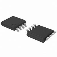
PCA8565TS/1,118 NXP Semiconductors, PCA8565TS/1,118 Datasheet - Page 17

PCA8565TS/1,118
Manufacturer Part Number
PCA8565TS/1,118
Description
IC CMOS RTC/CALENDAR 8-TSSOP
Manufacturer
NXP Semiconductors
Type
Clock/Calendarr
Datasheet
1.PCA8565TS1118.pdf
(39 pages)
Specifications of PCA8565TS/1,118
Package / Case
8-TSSOP
Time Format
HH:MM:SS (24 hr)
Date Format
YY-MM-DD-dd
Interface
I²C, 2-Wire Serial
Voltage - Supply
1.8 V ~ 5.5 V
Operating Temperature
-40°C ~ 125°C
Mounting Type
Surface Mount
Mounting Style
SMD/SMT
Lead Free Status / RoHS Status
Lead free / RoHS Compliant
Memory Size
-
Lead Free Status / Rohs Status
Lead free / RoHS Compliant
Other names
568-1902-2
935272132118
PCA8565TS-T
935272132118
PCA8565TS-T
Available stocks
Company
Part Number
Manufacturer
Quantity
Price
Company:
Part Number:
PCA8565TS/1,118
Manufacturer:
Freescale
Quantity:
77
Part Number:
PCA8565TS/1,118
Manufacturer:
NXP/恩智浦
Quantity:
20 000
NXP Semiconductors
PCA8565_2
Product data sheet
9.10 Voltage-low detector
9.11 External clock (EXT_CLK) test mode
Table 27.
[1]
The PCA8565 has an on-chip voltage-low detector. When V
the Seconds register is set to indicate that the integrity of the clock information is no
longer guaranteed. The VL flag is cleared using the interface.
Bit VL is intended to detect the situation when V
battery operation. Should V
This indicates that the time may be corrupt (see
A test mode is available which allows for on-board testing. In such a mode it is possible to
set up test conditions and control the operation of the RTC.
The test mode is entered by setting bit TEST1 in register Control_1. Then pin CLKOUT
becomes an input. The test mode replaces the internal 64 Hz signal with the signal
applied to pin CLKOUT. Every 64 positive edges applied to pin CLKOUT will then
generate an increment of one second.
Bit
7
6 to 2 -
1 to 0 FD[1:0]
Fig 9.
Default value.
Symbol
FE
Voltage-low detection
Register CLKOUT_control (address 0Dh) bits description
Rev. 02 — 16 June 2009
V
V
Value
0
1
-
00
01
10
11
DD
low
DD
[1]
[1]
reach V
Description
the CLKOUT output is inhibited and CLKOUT output is set
to high-impedance
the CLKOUT output is activated
unused
frequency output at pin CLKOUT
period of battery
operation
32.768 kHz
1.024 kHz
32 Hz
1 Hz
low
before power is re-asserted then bit VL is set.
DD
Figure
VL set
is decreasing slowly, for example under
normal power
operation
9).
mgr887
DD
t
drops below V
Real time clock/calendar
PCA8565
© NXP B.V. 2009. All rights reserved.
low
, bit VL in
17 of 39


