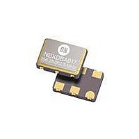
NBXDBA012LN1TAG ON Semiconductor, NBXDBA012LN1TAG Datasheet - Page 2

NBXDBA012LN1TAG
Manufacturer Part Number
NBXDBA012LN1TAG
Description
IC CLK OSC 106.25/212.5MHZ 6CLCC
Manufacturer
ON Semiconductor
Type
Clock Oscillatorr
Series
NBXr
Datasheet
1.NBXDBA012LN1TAG.pdf
(6 pages)
Specifications of NBXDBA012LN1TAG
Package / Case
6-CLCC
Voltage - Supply
3 V ~ 3.6 V
Frequency
106.25MHz/212.5MHz
Operating Temperature
-40°C ~ 85°C
Count
*
Frequency Stability
50 PPM
Termination Style
SMD/SMT
Supply Voltage
3.3 Volts
Supply Voltage (min)
2.97 Volts
Supply Voltage (max)
3.63 Volts
Dimensions
5 mm W x 7 mm L x 1.8 mm H
Minimum Operating Temperature
- 40 C
Maximum Operating Temperature
+ 85 C
Duty Cycle (max)
52 %
Mounting Style
SMD/SMT
Product
XO
Height
1.8 mm
Lead Free Status / RoHS Status
Lead free / RoHS Compliant
Available stocks
Company
Part Number
Manufacturer
Quantity
Price
Company:
Part Number:
NBXDBA012LN1TAG
Manufacturer:
ON Semiconductor
Quantity:
205
Part Number:
NBXDBA012LN1TAG
Manufacturer:
ON/安森美
Quantity:
20 000
Stresses exceeding Maximum Ratings may damage the device. Maximum Ratings are stress ratings only. Functional operation above the
Recommended Operating Conditions is not implied. Extended exposure to stresses above the Recommended Operating Conditions may affect
device reliability.
Table 2. OUTPUT ENABLE TRI−STATE FUNCTION
Table 1. PIN DESCRIPTION
Table 5. MAXIMUM RATINGS
Symbol
Pin No.
V
T
T
I
T
out
stg
DD
sol
A
1
2
3
4
5
6
HIGH Level
LOW Level
OE Pin
Positive Power Supply
LVPECL Output Current
Operating Temperature Range
Storage Temperature Range
Wave Solder
Open
Symbol
FSEL
GND
CLK
CLK
V
OE
DD
Table 4. ATTRIBUTES
1. For additional Moisture Sensitivity information, refer to Application Note AND8003/D.
Input Default State Resistor
ESD Protection
Meets or Exceeds JEDEC Standard EIA/JESD78 IC Latchup Test
LVTTL/LVCMOS
LVTTL/LVCMOS
LVPECL Output
LVPECL Output
Parameter
Power Supply
Power Supply
Control Input
Control Input
I/O
Characteristic
Output Pins
High Z
Active
Active
Figure 2. Pin Connections
Output Enable Pin. When left floating pin defaults to logic HIGH and output is active.
See OE pin description Table 2.
Output Frequency Select Pin. Pin will default to logic HIGH when left open. See Output
Frequency Select pin description Table 3.
Ground 0 V.
Non−Inverted Clock Output. Typically loaded with 50 W receiver termination resistor to
V
Non−Inverted Clock Output. Typically loaded with 50 W receiver termination resistor to
V
Positive power supply voltage. Voltage should not exceed 3.3 V ±10%.
Human Body Model
TT
TT
= V
= V
Machine Model
FSEL
GND
DD
DD
OE
http://onsemi.com
− 2 V.
− 2 V.
See Figure 8
1
2
3
Condition 1
Continuous
GND = 0 V
Surge
2
Table 3. OUTPUT FREQUENCY SELECT
6
5
4
V
CLK
CLK
(Top View)
(pin will float high)
DD
HIGH Level
LOW Level
FSEL Pin
Open
Description
Condition 2
170 kW
Value
200 V
2 kV
Output Frequency (MHz)
−55 to +120
−40 to +85
Rating
260
4.6
25
50
106.25
106.25
212.5
Units
mA
°C
°C
°C
V


