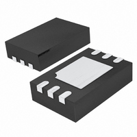
LTC6991IS6#TRPBF Linear Technology, LTC6991IS6#TRPBF Datasheet - Page 7

LTC6991IS6#TRPBF
Manufacturer Part Number
LTC6991IS6#TRPBF
Description
IC TIMERBLOX OSCILLATOR TSOT23-6
Manufacturer
Linear Technology
Datasheet
1.LTC6991CDCBTRMPBF.pdf
(24 pages)
Specifications of LTC6991IS6#TRPBF
Frequency
*
Voltage - Supply
*
Current - Supply
135µA
Operating Temperature
*
Package / Case
TSOT-23-6, TSOT-6
Count
*
Lead Free Status / RoHS Status
Lead free / RoHS Compliant
Available stocks
Company
Part Number
Manufacturer
Quantity
Price
Typical perForMance characTerisTics
V
pin FuncTions
V
ply should be kept free from noise and ripple. It should be
bypassed directly to the GND pin with a 0.1µF capacitor.
DIV (Pin 2/Pin 4): Programmable Divider and Polarity
Input. A V
pin voltage (V
V
and GND. Use 1% resistors to ensure an accurate result.
The DIV pin and resistors should be shielded from the
OUT pin or any other traces that have fast edges. Limit
the capacitance on the DIV pin to less than 100pF so that
V
mines the polarity of the RST and OUT pins. If POL = 0,
RST is active-high, and forces OUT low. If POL = 1, RST
is active-low and forces OUT high.
SET (Pin 3/Pin 3): Frequency-Setting Input. The voltage
on the SET pin (V
amount of current sourced from the SET pin (I
grams the master oscillator frequency. The I
range is 1.25µA to 20µA. The output oscillation will stop
if I
nected between SET and GND is the most accurate way to
set the frequency. For best performance, use a precision
metal or thin film resistor of 0.5% or better tolerance and
+
+
DIV
DIV
= 3.3V, R
SET
(Pin 1/Pin 5): Supply Voltage (2.25V to 5.5V). This sup-
may be generated by a resistor divider between V
settles quickly. The MSB of DIVCODE (POL) deter-
drops below approximately 500nA. A resistor con-
SET
+
referenced A/D converter monitors the DIV
= 200k, T
DIV
) to determine a 4-bit result (DIVCODE).
SET
50
45
40
35
30
25
20
15
10
5
0
2
Output Resistance
vs Supply Current
) is regulated to 1V above GND. The
A
OUTPUT SINKING CURRENT
= 25°C unless otherwise noted.
3
(DCB/S6)
SUPPLY VOLTAGE (V)
OUTPUT SOURCING CURRENT
4
5
SET
6991 G22
SET
current
6
) pro-
+
RST (Pin 4/Pin 1): Output Reset. The behavior of the RST
pin is dependent on the polarity bit (POL). The POL bit is
configured via the DIVCODE setting. When POL = 0, setting
RST high forces OUT low and setting RST low allows the
output to oscillate. When POL = 1, RST is active low. In
that case, setting RST low forces OUT high and setting
RST high allows the output to oscillate.
50ppm/°C or better temperature coefficient. For lower ac-
curacy applications an inexpensive 1% thick film resistor
may be used.
Limit the capacitance on the SET pin to less than 10pF
to minimize jitter and ensure stability. Capacitance less
than 100pF maintains the stability of the feedback circuit
regulating the V
1V/DIV
1V/DIV
OUT
V
+
Typical Start-Up with POL = 1
V
DIVCODE = 15
R
+
SET
= 2.5V
= 50k
V
500µs
+
R
SET
SET
RST
GND
SET
voltage.
LTC6991
250µs/DIV
1µs (t
INITIAL PULSE
OUT
6991 PF
MASTER
DIV
V
+
) WIDE
C1
0.1µF
6991 G19
V
LTC6991
+
R1
R2
6991f


