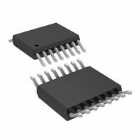
LTC6909IMS#PBF Linear Technology, LTC6909IMS#PBF Datasheet - Page 14

LTC6909IMS#PBF
Manufacturer Part Number
LTC6909IMS#PBF
Description
IC OSCILLATOR W/SS MOD 16-MSOP
Manufacturer
Linear Technology
Type
Oscillator, Siliconr
Datasheet
1.LTC6909CMSPBF.pdf
(22 pages)
Specifications of LTC6909IMS#PBF
Frequency
6.67MHz
Voltage - Supply
2.7 V ~ 5.5 V
Current - Supply
2.4mA
Operating Temperature
-40°C ~ 85°C
Package / Case
16-MSOP
Clock External Input
No
Supply Voltage Range
2.7V To 5.5V
Digital Ic Case Style
MSOP
No. Of Pins
16
Operating Temperature Range
-40°C To +85°C
Msl
MSL 1 - Unlimited
Rohs Compliant
Yes
Lead Free Status / RoHS Status
Lead free / RoHS Compliant
Count
-
Available stocks
Company
Part Number
Manufacturer
Quantity
Price
LTC6909
ApplicAtions inForMAtion
peak electromagnetic radiation (or conduction) is reduced.
Output ripple may be somewhat increased, but its behavior
is very much like noise and its system impact is benign.
SUPPLY BYPASSING, SIGNAL CONNECTIONS AND
PCB LAYOUT
Using the LTC6909 in spread spectrum mode naturally
eliminates any concerns for output frequency accuracy
and stability as it is continually hopping to new settings.
In fixed frequency applications however, some attention to
V
output frequency error. Ripple frequency components on
the supply line near the programmed output frequency of
the LTC6909 in excess of 30mV
tional 0.2% of frequency error. In applications where a fixed
frequency LTC6909 output clock is used to synchronize
the same switching regulator that provides the V
to the oscillator, noticeable jitter of the clock may occur if
the ripple exceeds 30mV
The LTC6909’s accuracy is affected as described above
by supply ripple on the V
sentially insensitive to supply ripple. The V
the power for the analog section of the LTC6909 and its
current is largely constant for a given R
The V
put drivers and its current requirement consists mainly of
large bursts that digital circuitry requires when switching.
The peak current required by the output drivers is by far
the largest. The current is mainly dependent on output
capacitive loading and the supply voltage.
Figure 6 shows how to connect the V
pins to the power supply as well as a suggested PCB layout.
The PCB layout assumes a two layer board with a ground
plane in the layer beneath the part and 0805 sized passive
components. The PCB layout in Figure 6 is a guide and
need not be followed exactly. However, there are several
items to note from the layout as follows:
1. There should be a ground plane underneath and around
14
+
the part. Connect the GND pin to this plane through
supply voltage ripple is required to minimize additional
+
D pin supplies the digital section including the out-
P-P
+
A pin only. The V
.
P-P
could create an addi-
+
A and V
SET
+
resistor value.
A pin supplies
+
D pin is es-
+
D supply
+
supply
2. Place the bypass capacitors, C1 and C2, as close to the
3. The connection to the V
4. Connect the bypass capacitors, C1 and C2, directly to the
5. Connect the R
6. Provide a ground shield around the R
7. Route the output signals, OUT1 through OUT8, away from
8. When using the LTC6909 with spread spectrum disabled,
multiple (three to four minimum) vias to minimize
inductance.
V
between the capacitor’s lead and the part’s pins.
supply should be through a low impedance path. If
the board has a V
top layer connection shown in Figure 6. Use multiple
vias (three to four minimum) at each point to connect
the V
inductance.
GND pin using a low inductance path. The connection
from C1 to the GND pin is easily done directly on the top
layer. The C2 path is more difficult but is accomplished
through multiple vias to the ground plane.
the V
through any manner other than directly to the V
will result greater frequency error.
its connections to V
high impedance point and is susceptible to interference
from noisy signal lines such as the part’s CMOS outputs
OUT1 through OUT8.
the SET pin as soon as possible to minimize coupling.
an active output is connected to the MOD pin. This is
best done by routing the OUT1 signal under the part
as shown in Figure 6. The ground shield between this
trace and the R
coupling of the OUT1 signal into the SET pin.
+
A and V
+
+
A and V
A pin. Connecting the resistor to the V
+
D pins as possible to minimize the inductance
+
SET
SET
D pins to the V
resistor is very important to minimize
+
resistor directly to the SET pin and
power plane, use it instead of the
+
A and SET. The SET pin is a fairly
+
A and V
+
plane to minimize the
+
D pins to the main
SET
resistor and
+
supply
+
A pin
6909fa


