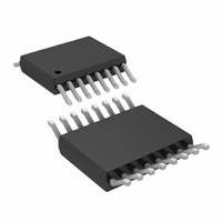
LTC6909IMS#PBF Linear Technology, LTC6909IMS#PBF Datasheet - Page 13

LTC6909IMS#PBF
Manufacturer Part Number
LTC6909IMS#PBF
Description
IC OSCILLATOR W/SS MOD 16-MSOP
Manufacturer
Linear Technology
Type
Oscillator, Siliconr
Datasheet
1.LTC6909CMSPBF.pdf
(22 pages)
Specifications of LTC6909IMS#PBF
Frequency
6.67MHz
Voltage - Supply
2.7 V ~ 5.5 V
Current - Supply
2.4mA
Operating Temperature
-40°C ~ 85°C
Package / Case
16-MSOP
Clock External Input
No
Supply Voltage Range
2.7V To 5.5V
Digital Ic Case Style
MSOP
No. Of Pins
16
Operating Temperature Range
-40°C To +85°C
Msl
MSL 1 - Unlimited
Rohs Compliant
Yes
Lead Free Status / RoHS Status
Lead free / RoHS Compliant
Count
-
Available stocks
Company
Part Number
Manufacturer
Quantity
Price
ApplicAtions inForMAtion
transitions have been slowed and the corners rounded
by a first order lowpass filter with a corner frequency set
to the modulation rate (f
tion rate divider setting, which is determined by the state
of the MOD pin. This filtered modulating signal may be
acceptable for many logic systems but the cycle-to-cycle
jitter issues must be considered carefully.
DRIVING SWITCHING REGULATORS
The LTC6909 is designed primarily to provide an accurate
and stable clock for switching regulator systems. The
CMOS logic outputs are suitable for directly driving most
switching regulators and switching controllers. Linear
Technology has a broad line of fully integrated switching
regulators and switching regulator controllers designed
for synchronization to an external clock. All of these
parts have one pin assigned for external clock input. The
nomenclature varies depending on the part’s family his-
tory. SYNC, PLLIN, SYNC/MODE, EXTCLK, FCB and S/S
(shorthand for SYNC/SHDN) are examples of clock input
pin names used with Linear Technology ICs.
For the best EMC performance, the LTC6909 should be run
with the MOD pin tied to ground (SSFM enabled, modula-
tion rate set to f
strictly specified bandwidths and conditions. Modulating
faster than, or as close to, the test bandwidth as possible
gives the lowest readings. The optimal modulating rate is
not as straightforward when the goal is to lower radiated
signal levels interfering with other circuitry in the system.
The modulation rate will have to be evaluated with the
specific system conditions to determine the optimal rate.
Depending on the specific frequency synchronization
method a switching regulator employs, the modulation
rate must be within the synchronization capability of the
regulator. Many regulators use a phase-locked loop (PLL)
for synchronization. For these parts, the PLL loop filter
should be designed to have sufficient capture range and
bandwidth.
The frequency hopping transitions of the LTC6909 are
slowed by a lowpass filter. The corner frequency of this
filter is set to the modulation rate (f
OUT
/16). Regulatory testing is done with
OUT
/N), where N is the modula-
OUT
/N), where N is
the modulation rate divider setting, which is determined
by the state of the MOD pin. The MOD pin should be tied
to ground for the N = 16 setting. Floating the MOD pin
selects N = 32. The MOD pin should be tied to V
N = 64 setting. This is an important feature when driving
a switching regulator. The switching regulator is itself
a servo loop with a bandwidth typically on the order of
1/10 to 1/20 of the operating frequency. When the clock
frequency’s transition is within the bandwidth of the switch-
ing regulator, the regulator’s output stays in regulation. If
the transition is too sharp, beyond the bandwidth of the
switching regulator, the regulator’s output will experience
a sharp jump and then settle back into regulation. If the
bandwidth of the regulator is sufficiently high, beyond
f
One aspect of the output voltage that will change is the
output ripple voltage. Every switching regulator has some
output ripple at the clock frequency. For most switching
regulator designs with fixed MOSFET’s, fixed inductor,
fixed capacitors, the amount of ripple will vary with the
regulator’s operating frequency (the main exception be-
ing hysteretic architecture regulators). An increase in
frequency results in lower ripple and a frequency decrease
gives more ripple. This is true for static frequencies or
dynamic frequency modulated systems. If the modulating
signal was a triangle wave, the regulator’s output would
have a ripple that is amplitude modulated by the triangle
wave. This repetitive signal on the power supply could
cause system problems by mixing with other desired
signals creating distortion. Depending on the switching
regulator’s inductor design and triangle wave frequency,
it may even result in an audible noise. The LTC6909 uses
a pseudorandom noise-like signal. On an oscilloscope, it
looks essentially noise-like of even amplitude. The signal
is broadband and any mixing issues are eliminated. Ad-
ditionally, the pseudorandom signal repeats at such a low
rate that it is well below the audible range.
The LTC6909 with the spread spectrum frequency modula-
tion enabled results in improved EMC performance. If the
bandwidth of the switching regulator is sufficient, not a
difficult requirement in most cases, the regulator’s regula-
tion, efficiency and load response are maintained while
OUT
/N, then there will not be any regulation issues.
LTC6909
+
13
for the
6909fa


