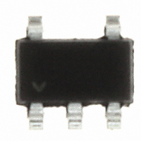
LTC6900CS5#TRMPBF Linear Technology, LTC6900CS5#TRMPBF Datasheet - Page 6

LTC6900CS5#TRMPBF
Manufacturer Part Number
LTC6900CS5#TRMPBF
Description
IC OSC PREC 1KHZ-20MHZ TSOT23-5
Manufacturer
Linear Technology
Type
Oscillator, Siliconr
Datasheet
1.LTC6900CS5TRMPBF.pdf
(12 pages)
Specifications of LTC6900CS5#TRMPBF
Frequency
20MHz
Voltage - Supply
2.7 V ~ 5.5 V
Current - Supply
920µA
Operating Temperature
-40°C ~ 85°C
Package / Case
TSOT-23-5, TSOT-5, TSOP-5
Lead Free Status / RoHS Status
Lead free / RoHS Compliant
Count
-
Other names
LTC6900CS5#TRMPBFTR
Available stocks
Company
Part Number
Manufacturer
Quantity
Price
LTC6900
OPERATION
As shown in the Block Diagram, the LTC6900’s master os-
cillator is controlled by the ratio of the voltage between the
V
pin. The voltage on the SET pin is forced to approximately
1.1V below V
voltage. This voltage is accurate to ± 8% at a particular
input current and supply voltage (see Figure 1).
A resistor R
“locks together” the voltage (V
variation. This provides the LTC6900’s high precision. The
master oscillation frequency reduces to:
The LTC6900 is optimized for use with resistors between
10k and 2M, corresponding to master oscillator frequen-
cies between 100kHz and 20MHz.
To extend the output frequency range, the master oscillator
signal may be divided by 1, 10 or 100 before driving OUT
6
+
and SET pins and the current (I
ƒ
MO
= 10MHz •
1.4
1.3
1.2
1.1
1.0
0.9
0.8
Figure 1. V
SET
0.1
+
, connected between the V
by the PMOS transistor and its gate bias
⎛
⎝ ⎜
V
1
+
20kΩ
R
= 3V
+
SET
– V
I
RES
V
SET
+
⎞
⎠ ⎟
10
= 5V
(μA)
Variation with I
+
– V
RES
100
SET
) is entering the SET
) and current, I
6900 F01
1000
+
RES
and SET pins,
RES
,
(Pin 5). The divide-by value is determined by the state of
the DIV input (Pin 4). Tie DIV to GND or drive it below 0.5V
to select ÷1. This is the highest frequency range, with the
master output frequency passed directly to OUT. The DIV
pin may be fl oated or driven to midsupply to select ÷10,
the intermediate frequency range. The lowest frequency
range, ÷100, is selected by tying DIV to V
within 0.4V of V
R
overlapping frequency ranges near 100kHz and 1MHz.
The CMOS output driver has an on resistance that is typi-
cally less than 100Ω. In the ÷1 (high frequency) mode,
the rise and fall times are typically 7ns with a 5V supply
and 11ns with a 3V supply. These times maintain a clean
square wave at 10MHz (20MHz at 5V supply). In the ÷10
and ÷100 modes, where the output frequency is much lower,
slew rate control circuitry in the output driver increases
the rise/fall times to typically 14ns for a 5V supply and
19ns for a 3V supply. The reduced slew rate lowers EMI
(electromagnetic interference) and supply bounce.
SET
, divider setting and output frequency, including the
10000
Figure 2. R
1000
100
10
1
1k
+
. Figure 2 shows the relationship between
DESIRED OUTPUT FREQUENCY (Hz)
÷100
10k
SET
vs Desired Output Frequency
÷10
100k
÷1
1M
10M
6900 F02
+
100M
or driving it to
6900fa


