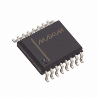
DS1023S-25+ Maxim Integrated Products, DS1023S-25+ Datasheet - Page 3

DS1023S-25+
Manufacturer Part Number
DS1023S-25+
Description
IC DELAY PROG 8BIT 0.25NS 16SOIC
Manufacturer
Maxim Integrated Products
Datasheet
1.DS1023S-25.pdf
(16 pages)
Specifications of DS1023S-25+
Number Of Taps/steps
256
Function
1-Shot
Delay To 1st Tap
16.5nS
Tap Increment
0.25nS
Available Total Delays
63.75ns
Voltage - Supply
4.75 V ~ 5.25 V
Operating Temperature
0°C ~ 70°C
Mounting Type
Surface Mount
Package / Case
16-SOIC (0.300", 7.5mm Width)
Propagation Delay Time
0.25 ns
Supply Voltage (min)
4.75 V
Operating Temperature Range
0 C to + 70 C
High Level Output Current
- 1 mA
Interface
Serial, Parallel
Logic Type
CMOS, TTL
Low Level Output Current
8 mA
Maximum Operating Temperature
+ 70 C
Minimum Operating Temperature
0 C
Mounting Style
SMD/SMT
Supply Voltage (max)
5.25 V
No. Of Taps
256
Delay Time Per Tap
250ns
Total Delay Time
63.75ns
Supply Voltage Range
4.75V To 5.25V
Digital Ic Case Style
SOIC
No. Of Pins
16
Rohs Compliant
Yes
Lead Free Status / RoHS Status
Lead free / RoHS Compliant
Number Of Independent Delays
-
Lead Free Status / Rohs Status
Lead free / RoHS Compliant
DS1023
Applications can read the setting of the DS1023 Delay Line by connecting the serial output pin (Q) to the
serial input (D) through a resistor with a value of 1 to 10 kohms (Figure 2). Since the read process is
destructive, the resistor restores the value read and provides isolation when writing to the device. The
resistor must connect the serial output (Q) of the last device to the serial input (D) of the first device of a
daisy chain (Figure 1). For serial readout with automatic restoration through a resistor, the device used to
write serial data must go to a high impedance state.
To initiate a serial read, latch enable (LE) is taken to a logic 1 while serial clock (CLK) is at a logic 0.
After a waiting time (t
), bit 7 (MSB) appears on the serial output (Q). On the first rising (0 --> 1)
EQV
transition of the serial clock (CLK), bit 7 (MSB) is rewritten and bit 6 appears on the output after a time
t
. To restore the input register to its original state, this clocking process must be repeated eight times.
CQV
In the case of a daisy chain, the process must be repeated eight times per package. If the value read is
restored before latch enable (LE) is returned to logic 0, no settling time (t
) is required and the
EDV
programmed delay remains unchanged.
Since the DS1023 is a CMOS design, unused input pins (P3 - P7) must be connected to well-defined logic
levels; they must not be allowed to float. Serial output Q/P0 should be allowed to float if unused.
CASCADING MULTIPLE DEVICES (DAISY CHAIN) Figure 1
SERIAL READOUT Figure 2
REFERENCE DELAY
In all delay lines there is an inherent, or “step zero”, delay caused by the propagation delay through the
input and output buffers. In this device the step zero delay can be quite large compared to the delay step
size. To simplify system design a reference delay has been included on chip which may be used to
compensate for the step zero delay. In practice this means that if the device is supplied with a clock, for
example, the minimum programmed output delay is effectively zero with respect to the reference delay.
3 of 16


