CY28442ZXC Cypress Semiconductor Corp, CY28442ZXC Datasheet - Page 7
CY28442ZXC
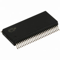
Manufacturer Part Number
CY28442ZXC
Description
IC CLOCK GEN ALVISO 56-TSSOP
Manufacturer
Cypress Semiconductor Corp
Type
Fanout Distribution, Spread Spectrum Clock Generatorr
Datasheet
1.CY28442ZXC.pdf
(22 pages)
Specifications of CY28442ZXC
Pll
Yes with Bypass
Input
LVTTL, Crystal
Output
Clock
Number Of Circuits
1
Ratio - Input:output
11:15
Differential - Input:output
No/Yes
Frequency - Max
200MHz
Divider/multiplier
Yes/No
Voltage - Supply
3.135 V ~ 3.465 V
Operating Temperature
0°C ~ 85°C
Mounting Type
Surface Mount
Package / Case
56-TSSOP II
Frequency-max
100MHz
Lead Free Status / RoHS Status
Lead free / RoHS Compliant
Available stocks
Company
Part Number
Manufacturer
Quantity
Price

Part Number:
CY28442ZXC-2
Manufacturer:
CYP
Quantity:
20 000
Company:
Part Number:
CY28442ZXC-2T
Manufacturer:
TI
Quantity:
11
Company:
Part Number:
CY28442ZXC-4
Manufacturer:
SEMTEC
Quantity:
946


Document #: 38-07680 Rev. **
Byte 5: Control Register 5 (continued)
Byte 6: Control Register 6
Byte 7: Vendor ID
Byte 8: Control Register 8
7
6
5
4
3
2
1
0
7
6
5
4
Bit
Bit
Bit
Bit
1
1
0
7
6
5
4
3
2
0
@Pup
@Pup
@Pup
@Pup
HW
HW
HW
0
0
0
0
0
1
1
0
0
0
0
1
0
0
0
0
1
0
0
CLKREQ#B
CLKREQ#B
CLKREQ#B
CLKREQ#B
Revision Code Bit 3
Revision Code Bit 2
Revision Code Bit 1
Revision Code Bit 0
Vendor ID Bit 3
Vendor ID Bit 2
Vendor ID Bit 1
Vendor ID Bit 0
PCI, PCIF and SRC clock
outputs except those set
to free running
TEST_MODE
RESERVED
TEST_SEL
CPU[T/C]1
CPU[T/C]0
Name
Name
Name
FS_C
Name
FS_B
FS_A
REF
ADVANCE INFORMATION
CPU[T/C]1 PWRDWN Drive Mode
0 = Driven when PD asserted,1 = Tri-state when PD asserted
CPU[T/C]0 PWRDWN Drive Mode
0 = Driven when PD asserted,1 = Tri-state when PD asserted
REF/N or Tri-state Select
0 = Tri-state, 1 = REF/N Clock
Test Clock Mode Entry Control
0 = Normal operation, 1 = REF/N or Tri-state mode,
RESERVED
REF Output Drive Strength
0 = Low, 1 = High
SW PCI_STP Function
0=SW PCI_STP assert, 1= SW PCI_STP deassert
When this bit is set to 0, all STOPPABLE PCI, PCIF and SRC outputs will
be stopped in a synchronous manner with no short pulses.
When this bit is set to 1, all STOPPED PCI, PCIF and SRC outputs will
resume in a synchronous manner with no short pulses.
FS_C Reflects the value of the FS_C pin sampled on power up
0 = FS_C was low during VTT_PWRGD# assertion
FS_B Reflects the value of the FS_B pin sampled on power up
0 = FS_B was low during VTT_PWRGD# assertion
FS_A Reflects the value of the FS_A pin sampled on power up
0 = FS_A was low during VTT_PWRGD# assertion
Revision Code Bit 3
Revision Code Bit 2
Revision Code Bit 1
Revision Code Bit 0
Vendor ID Bit 3
Vendor ID Bit 2
Vendor ID Bit 1
Vendor ID Bit 0
SRC[T/C]7CLKREQ#B control
1 = SRC[T/C]7 stoppable by CLKREQ#B pin
0 = SRC[T/C]7 not controlled by CLKREQ#B pin
SRC[T/C]5 CLKREQ#B control
1 = SRC[T/C]5 stoppable by CLKREQ#B pin
0 = SRC[T/C]5 not controlled by CLKREQ#B pin
SRC[T/C]3 CLKREQ#B control
1 = SRC[T/C]3 stoppable by CLKREQ#B pin
0 = SRC[T/C]3 not controlled by CLKREQ#B pin
SRC[T/C]1 CLKREQ#B control
1 = SRC[T/C]1 stoppable by CLKREQ#B pin
0 = SRC[T/C]1 not controlled by CLKREQ#B pin
Description
Description
Description
Description
CY28442
Page 7 of 22
[+] Feedback
Related parts for CY28442ZXC
Image
Part Number
Description
Manufacturer
Datasheet
Request
R

Part Number:
Description:
Manufacturer:
Cypress Semiconductor Corp
Datasheet:
Part Number:
Description:
Manufacturer:
Cypress Semiconductor Corp
Datasheet:
Part Number:
Description:
Manufacturer:
Cypress Semiconductor Corp
Datasheet:
Part Number:
Description:
Manufacturer:
Cypress Semiconductor Corp
Datasheet:
Part Number:
Description:
Manufacturer:
Cypress Semiconductor Corp
Datasheet: