CY7B9911V-5JXC Cypress Semiconductor Corp, CY7B9911V-5JXC Datasheet - Page 4
CY7B9911V-5JXC
Manufacturer Part Number
CY7B9911V-5JXC
Description
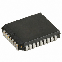
IC CLK BUFF SKEW 8OUT 32PLCC
Manufacturer
Cypress Semiconductor Corp
Type
Fanout Distribution, Zero Delay Bufferr
Series
RoboClock+™r
Datasheet
1.CY7B9911V-5JXC.pdf
(17 pages)
Specifications of CY7B9911V-5JXC
Number Of Circuits
1
Package / Case
32-PLCC
Pll
Yes
Input
LVTTL
Output
LVTTL
Ratio - Input:output
1:8
Differential - Input:output
No/No
Frequency - Max
110MHz
Divider/multiplier
Yes/Yes
Voltage - Supply
3 V ~ 3.6 V
Operating Temperature
0°C ~ 70°C
Mounting Type
Surface Mount
Frequency-max
110MHz
Output Frequency Range
3.75 MHz to 110 MHz
Supply Voltage (max)
3.63 V
Supply Voltage (min)
2.97 V
Maximum Operating Temperature
+ 70 C
Minimum Operating Temperature
0 C
Mounting Style
SMD/SMT
Operating Supply Voltage
3.3 V
Lead Free Status / RoHS Status
Lead free / RoHS Compliant
Lead Free Status / RoHS Status
Lead free / RoHS Compliant, Lead free / RoHS Compliant
Other names
428-2240-5
CY7B9911V-5JXC
CY7B9911V-5JXC
Available stocks
Company
Part Number
Manufacturer
Quantity
Price
Company:

Part Number:
CY7B9911V-5JXC
Manufacturer:
CY
Quantity:
23
Company:
Part Number:
CY7B9911V-5JXC
Manufacturer:
Cypress Semiconductor Corp
Quantity:
10 000
Company:
Part Number:
CY7B9911V-5JXCT
Manufacturer:
Cypress Semiconductor Corp
Quantity:
10 000


Document Number: 38-07408 Rev. *F
Block Diagram Description
Phase Frequency Detector and Filter
The Phase Frequency Detector and Filter blocks accept inputs
from the Reference Frequency (REF) input and the Feedback
(FB) input. They generate correction information to control the
frequency of the Voltage Controlled Oscillator (VCO). These
blocks, along with the VCO, form a Phase Locked Loop (PLL)
that tracks the incoming REF signal.
VCO and Time Unit Generator
The VCO accepts analog control inputs from the PLL filter block.
It generates a frequency used by the time unit generator to
create discrete time units that are selected in the skew select
matrix. The operational range of the VCO is determined by the
FS control pin. The time unit (t
frequency of the device and the level of the FS pin as shown in
Table
Table 1. Frequency Range Select and t
FS
LOW
MID
HIGH
Notes
1. For all three-state inputs, HIGH indicates a connection to V
2. The level to be set on FS is determined by the “normal” operating frequency (f
3. When the FS pin is selected HIGH, the REF input must not transition upon power up until V
[2, 3]
circuitry holds an unconnected input to V
(f
inputs is f
multiplication using a divided output as the FB input.
NOM
1.
) always appears at 1Q0 and the other outputs when they are operated in their undivided modes (see
f
Min
NOM
15
25
40
NOM
when the output connected to FB is undivided. The frequency of the REF and FB inputs is f
(MHz)
Max
110
30
50
t
U
where N =
=
----------------------- -
f
44
26
16
U
NOM
) is determined by the operating
1
×
N
CC
/2.
Frequency (MHz) At
Which t
U
Approximate
Calculation
22.7
38.5
62.5
U
CC
= 1.0 ns
, LOW indicates a connection to GND, and MID indicates an open connection. Internal termination
[1]
NOM
) of the V
Skew Select Matrix
The skew select matrix is comprised of four independent
sections. Each section has two low skew, high fanout drivers
(xQ0, xQ1), and two corresponding three level function select
(xF0, xF1) inputs.
functions for each section as determined by the function select
inputs. All times are measured with respect to the REF input
assuming that the output connected to the FB input has 0t
selected.
Table 2. Programmable Skew Configurations
1F1, 2F1,
LOW
LOW
LOW
MID
MID
MID
HIGH
HIGH
HIGH
3F1, 4F1
Function Selects
CO
and Time Unit Generator
CC
has reached 2.8 V.
1F0, 2F0,
LOW
MID
HIGH
LOW
MID
HIGH
LOW
MID
HIGH
3F0, 4F0
NOM
Table 2
/2 or f
Table
NOM
2). The frequency appearing at the REF and FB
1Q0, 1Q1,
2Q0, 2Q1
shows the nine possible output
(seeLogic Block
/4 when the part is configured for a frequency
–4t
–3t
–2t
–1t
+1t
+2t
+3t
+4t
0t
3.3 V RoboClock+™
U
U
U
U
U
U
U
U
U
Output Functions
Divide by 2 Divide by 2
Divide by 4
3Q0, 3Q1
Diagram). Nominal frequency
–6t
–4t
–2t
+2t
+4t
+6t
0t
U
U
U
U
U
U
U
CY7B9911V
[1]
4Q0, 4Q1
Page 4 of 17
Inverted
–6t
–4t
–2t
+2t
+4t
+6t
0t
U
U
U
U
U
U
U
U
[+] Feedback
Related parts for CY7B9911V-5JXC
Image
Part Number
Description
Manufacturer
Datasheet
Request
R

Part Number:
Description:
IC CLK BUFF SKEW 8OUT 32PLCC
Manufacturer:
Cypress Semiconductor Corp
Datasheet:

Part Number:
Description:
CY7B9911V-5JXCT
Manufacturer:
Cypress Semiconductor Corp
Datasheet:
Part Number:
Description:
IC CLK BUFF SKEW 8OUT 32PLCC
Manufacturer:
Cypress Semiconductor Corp
Datasheet:
Part Number:
Description:
IC CLK BUFF SKEW 8OUT 32PLCC
Manufacturer:
Cypress Semiconductor Corp
Datasheet:

Part Number:
Description:
Manufacturer:
Cypress Semiconductor Corp
Datasheet:
Part Number:
Description:
Manufacturer:
Cypress Semiconductor Corp
Datasheet:
Part Number:
Description:
Manufacturer:
Cypress Semiconductor Corp
Datasheet: