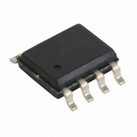
CY2304SXC-2 Cypress Semiconductor Corp, CY2304SXC-2 Datasheet - Page 5

CY2304SXC-2
Manufacturer Part Number
CY2304SXC-2
Description
IC CLK ZDB 4OUT 133MHZ 8SOIC
Manufacturer
Cypress Semiconductor Corp
Type
Fanout Distribution, Zero Delay Bufferr
Datasheet
1.CY2304SXC-2.pdf
(15 pages)
Specifications of CY2304SXC-2
Number Of Circuits
1
Package / Case
8-SOIC (3.9mm Width)
Pll
Yes
Input
Clock
Output
Clock
Ratio - Input:output
1:4
Differential - Input:output
No/No
Frequency - Max
133.3MHz
Divider/multiplier
Yes/Yes
Voltage - Supply
3 V ~ 3.6 V
Operating Temperature
0°C ~ 70°C
Mounting Type
Surface Mount
Frequency-max
133MHz
Output Frequency Range
10 MHz to 133.3 MHz
Supply Voltage (max)
3.6 V
Supply Voltage (min)
3 V
Maximum Operating Temperature
+ 70 C
Minimum Operating Temperature
0 C
Mounting Style
SMD/SMT
Operating Supply Voltage
3.3 V
Clock Ic Type
Clock Buffer
Frequency
133.33MHz
No. Of Outputs
4
No. Of Multipliers / Dividers
1
Supply Current
45mA
Supply Voltage Range
3V To 3.6V
Digital Ic Case Style
SOIC
No. Of Pins
8
Rohs Compliant
Yes
Lead Free Status / RoHS Status
Lead free / RoHS Compliant
Lead Free Status / RoHS Status
Lead free / RoHS Compliant, Lead free / RoHS Compliant
Other names
428-2894-5
CY2304SXC-2
CY2304SXC-2
Maximum Ratings
Supply voltage to ground potential.................–0.5 V to +7.0 V
DC input voltage (except Ref)...............–0.5 V to V
DC input voltage REF.............................................–0.5 V to 7 V
Operating Conditions for CY2304SXC Commercial Temperature Devices
Electrical Characteristics for CY2304SXC Commercial Temperature Devices
Document Number: 38-07247 Rev. *J
Notes
V
T
C
C
t
V
V
I
I
V
V
I
I
3. Applies to both REF clock and FBK.
4. Parameter is guaranteed by design and characterization. Not 100% tested in production.
PU
IL
IH
DD
DD
A
DD
IL
IH
OL
OH
L
IN
Parameter
Parameter
(PD mode) Power-down supply current REF = 0 MHz
Supply voltage
Operating temperature (ambient temperature)
Load capacitance (below 100 MHz)
Load capacitance (from 100 MHz to 133 MHz)
Input capacitance
Power-up time for all V
(power ramps must be monotonic)
Input LOW voltage
Input HIGH voltage
Input LOW current
Input HIGH current
Output LOW voltage
Output HIGH voltage
Supply current
Description
[3]
[4]
[4]
DD
s to reach minimum specified voltage
Description
V
V
I
I
Unloaded outputs, 100 MHz REF, Select
inputs at V
Unloaded outputs, 66 MHz REF (–1,–2)
Unloaded outputs, 33 MHz REF (–1,–2)
OL
OH
IN
IN
= 8 mA (–1, –2)
= 0 V
= V
= –8 mA (–1, –2)
DD
+ 0.5 V
DD
DD
Test Conditions
or GND
Storage temperature ..................................–65 °C to +150 °C
Junction temperature ..................................................150 °C
Static discharge voltage
(per MIL-STD-883, Method 3015).............................> 2000 V
0.05
Min
Min
3.0
2.0
2.4
0
–
–
–
–
–
–
–
–
–
–
–
100.0
Max
Max
50.0
45.0
12.0
32.0
18.0
3.6
0.8
0.4
70
30
15
50
7
–
–
CY2304
Page 5 of 15
Unit
Unit
ms
mA
mA
mA
°C
pF
pF
pF
A
A
A
V
V
V
V
V
[+] Feedback


