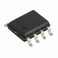
CY2304SXC-2 Cypress Semiconductor Corp, CY2304SXC-2 Datasheet - Page 3

CY2304SXC-2
Manufacturer Part Number
CY2304SXC-2
Description
IC CLK ZDB 4OUT 133MHZ 8SOIC
Manufacturer
Cypress Semiconductor Corp
Type
Fanout Distribution, Zero Delay Bufferr
Datasheet
1.CY2304SXC-2.pdf
(15 pages)
Specifications of CY2304SXC-2
Number Of Circuits
1
Package / Case
8-SOIC (3.9mm Width)
Pll
Yes
Input
Clock
Output
Clock
Ratio - Input:output
1:4
Differential - Input:output
No/No
Frequency - Max
133.3MHz
Divider/multiplier
Yes/Yes
Voltage - Supply
3 V ~ 3.6 V
Operating Temperature
0°C ~ 70°C
Mounting Type
Surface Mount
Frequency-max
133MHz
Output Frequency Range
10 MHz to 133.3 MHz
Supply Voltage (max)
3.6 V
Supply Voltage (min)
3 V
Maximum Operating Temperature
+ 70 C
Minimum Operating Temperature
0 C
Mounting Style
SMD/SMT
Operating Supply Voltage
3.3 V
Clock Ic Type
Clock Buffer
Frequency
133.33MHz
No. Of Outputs
4
No. Of Multipliers / Dividers
1
Supply Current
45mA
Supply Voltage Range
3V To 3.6V
Digital Ic Case Style
SOIC
No. Of Pins
8
Rohs Compliant
Yes
Lead Free Status / RoHS Status
Lead free / RoHS Compliant
Lead Free Status / RoHS Status
Lead free / RoHS Compliant, Lead free / RoHS Compliant
Other names
428-2894-5
CY2304SXC-2
CY2304SXC-2
Pinout
Table 2. Pin Definitions - 8-pin SOIC
Document Number: 38-07247 Rev. *J
l
Notes
1. Weak pull-down.
2. Weak pull-down on all outputs.
Pin
1
2
3
4
5
6
7
8
CLKA1
CLKA2
CLKB1
CLKB2
Signal
REF
GND
FBK
V
DD
[1]
[2]
[2]
[2]
[2]
Figure 1. 8-pin SOIC - Top View
CLKA1
CLKA2
GND
REF
Input reference frequency, 5 V tolerant input
Clock output, Bank A
Clock output, Bank A
Ground
Clock output, Bank B
Clock output, Bank B
3.3 V supply
PLL feedback input
1
2
3
4
8
7
6
5
V
CLKB1
FBK
CLKB2
DD
Description
CY2304
Page 3 of 15
[+] Feedback


