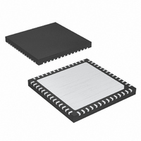
MAX3886ETN+ Maxim Integrated Products, MAX3886ETN+ Datasheet - Page 11

MAX3886ETN+
Manufacturer Part Number
MAX3886ETN+
Description
IC MULTIRATE CDR SER/DES56-TQFN
Manufacturer
Maxim Integrated Products
Type
Clock and Data Recovery (CDR)r
Datasheet
1.MAX3886ETN.pdf
(17 pages)
Specifications of MAX3886ETN+
Input
CML, LVDS
Output
CMOS, LVDS
Frequency - Max
622MHz, 2.488GHz
Voltage - Supply
3 V ~ 3.6 V
Operating Temperature
-40°C ~ 85°C
Mounting Type
Surface Mount
Package / Case
56-TQFN
Frequency-max
622MHz, 2.488GHz
Lead Free Status / RoHS Status
Lead free / RoHS Compliant
To minimize PON overhead, it is important that the laser
driver burst-enable (BEN) signal correspond accurately
with the beginning of the serial data burst. This is sup-
ported in the MAX3886 by the BENI LVDS input and
associated signal path. The LVDS burst-enable signal
from the MAC layer IC is passed through the same FIFO
as the parallel data and output on the BENO CML out-
put, which ensures that the laser driver’s burst enable
matches the beginning of the associated serial MSB. If
FRST or FERR are high, the BENO output is forced low
to prevent the laser driver from transmitting erroneous
data. The parallel data setup and hold timing require-
ments also apply to the burst-enable signal.
The lock detector operates by comparing a divided-
down version of the VCO output to the reference clock.
The LOCK output pin indicates lock (high) when the fre-
quency difference between the reference clock and the
CDR VCO is less than 250ppm, within the “pullin” range
of the PLL. The LOCK output indicates out-of-lock (low)
when the frequency difference between the reference
clock and the CDR VCO becomes more than 500ppm.
When valid input data is present, this provides a stable
lock indication.
Table 2. Clock and Data Rate Controls
MVCO
Open
Open
Open
Open
Multirate CDR with Integrated Serializer/Deserializer
0
0
0
0
1
1
1
1
MSYM
Burst-Enable Signal Processing
0
0
1
1
0
0
1
1
0
0
1
1
______________________________________________________________________________________
MDDR
Lock Detector Output
0
1
0
1
0
1
0
1
0
1
0
1
for GPON and BPON ONT Applications
SDI RATE
(Mbps)
1244
1244
1244
1244
2488
2488
2488
2488
622
622
622
622
PDO RATE
(Mbps)
155
155
155
155
311
311
311
311
622
622
622
622
Rx
At power-up, the CDR takes approximately 50ms (if
valid NRZ data is present) for initial acquisition while
the internal reference oscillator, the PLL, and the fre-
quency detector reach their operating conditions.
During this startup period, the LOCK status output may
provide false indication of a lock condition. Once the
PLL and frequency detector are initialized, the nominal
time for reacquisition of an NRZ input is 2ms.
When valid NRZ input data is not present, the lock
detector may produce a chattering LOCK indicator out-
put while the PLL searches for the input frequency. If
needed, an external digital filter can be used to mask
this chattering.
Table 1. Lock Detector Output
Table 2 summarizes the clock and data rates as con-
trolled by MVCO, MSYM, and MDDR.
PCKO
(MHz)
155
155
311
155
311
155
622
311
622
311
78
78
Valid NRZ data
No CDR input
CDR INPUT
SDO RATE
(Mbps)
1244
1244
1244
1244
2488
2488
155
155
622
622
622
622
PDI RATE
(Mbps)
155
155
155
155
311
311
311
311
622
622
39
39
Control Input Summary
Tx
LOCK OUTPUT
(MHz)
PCKI
155
155
155
155
311
311
311
311
622
622
0/1 (chatter)
39
39
1
RCKO
(MHz)
155
155
155
155
311
311
311
311
622
622
39
39
11


