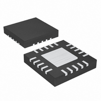
MAX3991UTG+ Maxim Integrated Products, MAX3991UTG+ Datasheet - Page 2

MAX3991UTG+
Manufacturer Part Number
MAX3991UTG+
Description
IC DATA RECOVERY W/AMP 24-TQFN
Manufacturer
Maxim Integrated Products
Type
Clock and Data Recovery (CDR)r
Datasheet
1.MAX3991UTG.pdf
(12 pages)
Specifications of MAX3991UTG+
Input
CML
Output
CML
Frequency - Max
693MHz
Voltage - Supply
3 V ~ 3.6 V
Operating Temperature
0°C ~ 85°C
Mounting Type
Surface Mount
Package / Case
24-TQFN Exposed Pad
Frequency-max
693MHz
Lead Free Status / RoHS Status
Lead free / RoHS Compliant
ABSOLUTE MAXIMUM RATINGS
Supply Voltage, V
Input Voltage Levels
CML Output Voltage
10Gbps Clock and Data Recovery
with Limiting Amplifier
ELECTRICAL CHARACTERISTICS
(See Table 1 for operating conditions. Typical values at V
Stresses beyond those listed under “Absolute Maximum Ratings” may cause permanent damage to the device. These are stress ratings only, and functional
operation of the device at these or any other conditions beyond those indicated in the operational sections of the specifications is not implied. Exposure to
absolute maximum rating conditions for extended periods may affect device reliability.
2
Supply Current
DATA INPUT SPECIFICATION (SDI±)
Single-Ended Input Resistance
Differential Input Resistance
Single-Ended Input Resistance
Matching
Differential Input Return Loss
DC Cancellation Loop Low-
Frequency Cutoff
REFERENCE CLOCK SPECIFICATION (REFCLK±)
Single-Ended Input Resisitance
Differential Input Resistance
CML OUTPUT SPECIFICATION (SDO±)
SDO± Differential Output Swing
SDO± Output Common-Mode
Voltage
SCLKO± Differential Output
Single-Ended Output Resistance
Differential Output Resistance
Single-Ended Output Resistance
Matching
Differential Output Return Loss
Common-Mode Output Return
Rise/Fall Time
Output AC Common Mode
Power-Down Assert Time
(SDI+, SDI-, REFCLK+,
REFCLK-) ....................................(V
(SDO+, SDO-, SCLKO+,
SLCKO-) ......................................(V
_______________________________________________________________________________________
PARAMETER
CC
..............................................-0.5V to +4.0V
CC
CC
SYM B O L
SDD11
SDD22
SCC22
R
I
- 1.0V) to (V
- 1.0V) to (V
R
R
CC
SE
D
O
0.1GHz to 5.5GHz (Note 1)
5.5GHz to 12GHz (Note 1)
(Note 2)
RL = 50Ω to V
0.1GHz to 5.5GHz (Note 1)
5.5GHz to 12GHz (Note 1)
0.1GHz to 15GHz (Note 1)
(20% to 80%) (Note 2)
(Note 2)
(Note 3)
CC
CC
+ 0.5V)
+ 0.5V)
CC
= +3.3V, T
CC
CONDITIONS
Voltage at (CFIL, LOL, VTH, POL,
Continuous Power Dissipation (T
Junction Temperature Range ............................-40°C to +150°C
Storage Temperature Range.............…………..-55°C to +150°C
Lead Temperature (soldering, 10s) ..……………………..+300°C
A
LOS, FCTL1, FCTL2) ..............................-0.5V to (V
24-Pin QFN (derate 20.8mW/°C above +85°C) .........1355mW
= +25°C, unless otherwise noted.)
MIN
168
575
42
84
84
42
84
18
A
=
+85°C)
V
TYP
12.5
0.16
106
100
100
200
650
380
100
CC
50
30
50
13
23
6
8
5
-
MAX
140
116
116
232
725
116
±5
±5
58
58
30
10
50
CC
mV
UNITS
mV
mV
+ 0.5V)
kHz
mA
dB
dB
dB
ps
µs
%
%
Ω
Ω
Ω
Ω
Ω
Ω
V
RMS
P-P
P-P


