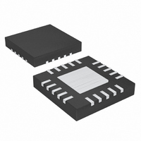
MAX3991UTG+ Maxim Integrated Products, MAX3991UTG+ Datasheet

MAX3991UTG+
Specifications of MAX3991UTG+
Related parts for MAX3991UTG+
MAX3991UTG+ Summary of contents
Page 1
... XFI-Compliant Output Interface ♦ LOS Indicator with Programmable Threshold ♦ LOL Indicator ♦ Power Dissipation: 350mW PART MAX3991UTG MAX3991UTG+* *Future product—contact factory for availability. +Denotes lead-free package. Applications TOP VIEW *THE EXPOSED PAD MUST BE CONNECTED TO CIRCUIT-BOARD GROUND FOR PROPER THERMAL AND ELECTRICAL PERFORMANCE. ...
Page 2
Clock and Data Recovery with Limiting Amplifier ABSOLUTE MAXIMUM RATINGS Supply Voltage, V ..............................................-0.5V to +4.0V CC Input Voltage Levels (SDI+, SDI-, REFCLK+, REFCLK-) ....................................(V CC CML Output Voltage (SDO+, SDO-, SCLKO+, SLCKO-) ......................................(V CC Stresses beyond those listed ...
Page 3
ELECTRICAL CHARACTERISTICS (continued) (See Table 1 for operating conditions. Typical values at V PARAMETER JITTER SPECIFICATION Jitter Peaking Jitter Transfer Bandwidth Sinusoidal Jitter Tolerance Jitter Generation Serial Data Output Deterministic Jitter PLL ACQUISITION/LOCK SPECIFICATION Acquisition Time LOL Assert Time Maximum ...
Page 4
Clock and Data Recovery with Limiting Amplifier ELECTRICAL CHARACTERISTICS (continued) (See Table 1 for operating conditions. Typical values at V Note 1: Measured with 100mV differential amplitude. P-P Note 2: Guaranteed by design and characterization. Note 3: Measured from ...
Page 5
Figure 1. RX LOL Assert and PLL Acquisition Time DATA INPUT POWER LOS ASSERT TIME LOS LOL Figure 2. LOS Assert/Deassert Time _______________________________________________________________________________________ 10Gbps Clock and Data Recovery with Limiting Amplifier ∆f/f REFCLK 651ppm 500ppm LOL ASSERT TIME LOL *ASSERT ...
Page 6
Clock and Data Recovery with Limiting Amplifier (V = 3.3V +25°C, unless otherwise noted MAX3991 OUPTUT AFTER XFP CONNECTOR 31 (INPUT = 9.95328Gbps PATTERN, 10mV MAX3991 toc01 20ps/div SUPPLY-INDUCED OUTPUT JITTER 0.07 0.06 ...
Page 7
T = +25°C, unless otherwise noted SDD22 vs. FREQUENCY XFI -5 -10 -15 -20 -25 -30 -35 -40 100M 1G 10G FREQUENCY (mHz) PIN NAME 1, 6, 11, 13 +3.3V ...
Page 8
Clock and Data Recovery with Limiting Amplifier PIN NAME Positive Reference Clock Input, Digital. The REFCLK inputs are designed to be AC-coupled to the reference clock source. REFCLK± have a 200Ω differential impedance. See the Detailed Description 21 REFCLK+ ...
Page 9
The integrated PLL recovers a synchronous clock, which is used to retime the input data. Connect a 0.047µF capacitor between CFIL and V PLL dampening. The external reference connected to REFCLK aids in frequency acquisition. Because the ref- erence clock ...
Page 10
Clock and Data Recovery with Limiting Amplifier 50Ω REFERENCE CLOCK 50Ω TRANSCEIVER TERMINATION Figure 5. Reference Clock Termination Table 3. Functional Control FCTL1 FCTL2 DESCRIPTION Normal operation, serial clock output 0 0 disabled Standby power-down mode. 0 ...
Page 11
VCC 50Ω 50Ω GND Figure 7. CML Output Model (SDI+) - (SDI-) (SDO+) - (SDO-) POL = VCC (SDO+) - (SDO-) POL = GND Figure 8. Polarity (POL) Function ______________________________________________________________________________________ 10Gbps Clock and Data Recovery with Limiting Amplifier SDO+ SDO- ...
Page 12
... Maxim cannot assume responsibility for use of any circuitry other than circuitry entirely embodied in a Maxim product. No circuit patent licenses are implied. Maxim reserves the right to change the circuitry and specifications without notice at any time. 12 ____________________Maxim Integrated Products, 120 San Gabriel Drive, Sunnyvale, CA 94086 408-737-7600 © 2005 Maxim Integrated Products V CC 0.047µ ...


