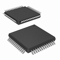
CY29976AXI Cypress Semiconductor Corp, CY29976AXI Datasheet - Page 6

CY29976AXI
Manufacturer Part Number
CY29976AXI
Description
IC CLK ZDB 12OUT 125MHZ 52LQFP
Manufacturer
Cypress Semiconductor Corp
Type
Zero Delay Bufferr
Datasheet
1.CY29976AXI.pdf
(9 pages)
Specifications of CY29976AXI
Package / Case
52-LQFP
Frequency - Max
125MHz
Voltage - Supply
3 V ~ 3.6 V
Operating Temperature
-40°C ~ 85°C
Mounting Type
Surface Mount
Frequency-max
125MHz
Number Of Circuits
1
Maximum Input Frequency
480 MHz
Minimum Input Frequency
200 MHz
Output Frequency Range
125 MHz
Supply Voltage (max)
3.63 V
Supply Voltage (min)
2.97 V
Maximum Operating Temperature
+ 85 C
Minimum Operating Temperature
- 40 C
Mounting Style
SMD/SMT
Operating Supply Voltage
3.3 V
Lead Free Status / RoHS Status
Contains lead / RoHS non-compliant
Output
-
Input
-
Lead Free Status / Rohs Status
Lead free / RoHS Compliant
Available stocks
Company
Part Number
Manufacturer
Quantity
Price
Company:
Part Number:
CY29976AXI
Manufacturer:
Microchip
Quantity:
2 354
Company:
Part Number:
CY29976AXI
Manufacturer:
Cypress Semiconductor Corp
Quantity:
10 000
Company:
Part Number:
CY29976AXIT
Manufacturer:
Cypress Semiconductor Corp
Quantity:
10 000
Power Management
The individual output enable/freeze control of the CY29976
allows the user to implement unique power management
schemes into the design. The outputs are stopped in the logic ‘0’
state when the freeze control bits are activated. The serial input
register contains one programmable freeze enable bit for 12 of
the 14 output clocks. The QC0 and FB_OUT outputs can not be
frozen with the serial port, this avoids any potential lock up
situation must an error occur in the loading of the serial data. An
output is frozen when a logic ‘0’ is programmed and enabled
Maximum Ratings
Input Voltage Relative to V
Input Voltage Relative to V
Storage Temperature: .............................. –65 C to + 150 C
Operating Temperature:.............................. –40 C to +85 C
Maximum Power Supply:................................................ 5.5V
DC Parameters
Document #: 38-07413 Rev. *D
Notes
V
V
V
V
I
I
V
V
I
I
C
3. Multiple Supplies: The voltage on any input or IO pin cannot exceed the power pin during power up. Power supply sequencing is NOT required.
4. The V
5. Inputs have pull up/pull down resistors that effect input current.
6. Driving series or parallel terminated 50 (or 50 to V
IL
IH
DDC
DD
Parameter
IL
IH
PP
CMR
OL
OH
in
input lies within the V
CMR
is the difference from the most positive side of the differential input signal. Normal operation is obtained when “High” input is within the V
Input Low Voltage
Input High Voltage
Peak-to-Peak Input Voltage PECL_CLK
Common Mode Range PECL_CLK
Input Low Current (at V
Input High Current (at V
Output Low Voltage
Output High Voltage
Quiescent Supply Current
PLL Supply Current
Input Pin Capacitance
PP
V
specification.
DD
[3]
SS
DD
= V
: ............................. V
: ............................. V
DDC
Description
D0-D3 are the control bits for QA0-QA3, respectively
D4-D7 are the control bits for QB0-QB3, respectively
D8-D10 are the control bits for QC1-QC3, respectively
D11 is the control bit for SYNC
= 3.3V ±10%, T
Start
Bit
IL
IH
= V
= V
D0 D1 D2 D3 D4 D5 D6 D7 D8 D9 D10 D11
SS
DD
DD
)
)
/2) transmission lines.
DD
SS
A
Figure 2. Control Bit Map
= –40 C to +85 C
– 0.3V
+ 0.3V
Note 4
V
Note 5
Note 5
I
I
All V
OL
OH
DD
= 20 mA, Note 6
= –20 mA, Note 6
when a logic ‘1’ is written. The enabling and freezing of individual
outputs is done in such a manner as to eliminate the possibility
of partial “runt” clocks.
The serial input register is programmed through the SDATA input
by writing a logic ‘0’ start bit followed by 12 NRZ freeze enable
bits. The period of each SDATA bit equals the period of the free
running SCLK signal. The SDATA is sampled on the rising edge
of SCLK.
This device contains circuitry to protect the inputs against
damage due to high static voltages or electric field; however,
precautions must be taken to avoid application of any voltage
higher than the maximum rated voltages to this circuit. For proper
operation, V
V
Unused inputs must always be tied to an appropriate logic
voltage level (either V
DDC
only
SS
Conditions
< (V
and V
in
or V
DD
in
and V
out
) < V
out
SS
DD
must be constrained to the range:
V
or V
DD
Min
V
300
2.0
2.4
SS
DD
– 2.0
).
Typ
10
4
V
DD
1000
–120
Max
V
120
0.8
0.5
15
15
CY29976
CMR
DD
– 0.6
Page 6 of 9
range and the
Unit
mV
mA
mA
µA
µA
pF
V
V
V
V
V
[+] Feedback


