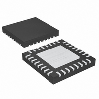
MAX3872ETJ+ Maxim Integrated Products, MAX3872ETJ+ Datasheet - Page 8

MAX3872ETJ+
Manufacturer Part Number
MAX3872ETJ+
Description
IC DATA RECOVERY W/AMP 32-TQFN
Manufacturer
Maxim Integrated Products
Type
Clock and Data Recovery (CDR)r
Datasheet
1.MAX3872ETJ.pdf
(15 pages)
Specifications of MAX3872ETJ+
Input
CML
Output
CML
Frequency - Max
2.67GHz
Voltage - Supply
3 V ~ 3.6 V
Operating Temperature
-40°C ~ 85°C
Mounting Type
Surface Mount
Package / Case
32-TQFN Exposed Pad
Frequency-max
2.67GHz
Lead Free Status / RoHS Status
Lead free / RoHS Compliant
The MAX3872 consists of a fully integrated phase-
locked loop (PLL), limiting amplifier with threshold
adjust, DC-offset cancellation loop, data retiming block,
and CML output buffers (Figure 5). The PLL consists of
a phase/frequency detector, a loop filter, and a voltage-
controlled oscillator (VCO) with programmable dividers.
This device is designed to deliver the best combination
of jitter performance and power dissipation by using a
fully differential signal architecture and low-noise
design techniques.
The SDI inputs of the MAX3872 accept serial NRZ data
with a differential input amplitude from 10mV
to1600mV
the jitter tolerance is met for a BER of 10
old adjust disabled. The input sensitivity can be as low
as 4mV
MAX3872 inputs are designed to directly interface with
a transimpedance amplifier such as the MAX3745.
For applications in which vertical threshold adjustment
is needed, the MAX3872 can be connected to the out-
put of an AGC amplifier such as the MAX3861. When
using the threshold adjust, the input voltage range is
50mV
tion for decision threshold adjust.
Multirate Clock and Data Recovery
with Limiting Amplifier
Figure 5. Functional Diagram
8
_______________________________________________________________________________________
P-P
FREFSET
P-P
to 600mV
P-P
V
SLBI+
SLBI-
LREF
SDI+
CTRL
SDI-
SIS
and still maintain a BER of 10
. The input sensitivity is 10mV
P-P
THRESHOLD
AMP
AMP
ADJUST
. See the Design Procedure sec-
Detailed Description
CAZ+
CANCELLATION
DC-OFFSET
LOGIC
SDI Input Amplifier
LOOP
CAZ-
-10
P-P
MAX3872
with thresh-
0
1
, at which
-10
P-P
. The
FREQUENCY
up
PHASE AND
DETECTOR
LOL
The SLBI input amplifier accepts either NRZ loopback
data or a reference clock signal. This amplifier can
accept a differential input amplitude from 50mV
800mV
The phase detector incorporated in the MAX3872 pro-
duces a voltage proportional to the phase difference
between the incoming data and the internal clock.
Because of its feedback nature, the PLL drives the
error voltage to zero, aligning the recovered clock to
the center of the incoming data eye for retiming.
The digital frequency detector (FD) acquires frequency
lock without the use of an external reference clock. The
frequency difference between the received data and
the VCO clock is derived by sampling the in-phase and
quadrature VCO outputs on both edges of the data
input signal. Depending on the polarity of the frequency
difference, the FD drives the VCO until the frequency
difference is reduced to zero. Once frequency acquisi-
tion is complete, the FD returns to a neutral state. False
locking is completely eliminated by this digital frequency
detector.
FILTER
LOOP
FIL
P-P
.
VCO
RATESET
RS1
÷ BY
N
D
REFERENCE
RS2
BANDGAP
V
REF
Q
SLBI Input Amplifier
Frequency Detector
CML
CML
Phase Detector
SDO+
SDO-
SCLKO+
SCLKO-
P-P
to


