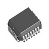
IDT82V1671J IDT, Integrated Device Technology Inc, IDT82V1671J Datasheet - Page 50

IDT82V1671J
Manufacturer Part Number
IDT82V1671J
Description
Manufacturer
IDT, Integrated Device Technology Inc
Datasheet
1.IDT82V1671J.pdf
(107 pages)
Specifications of IDT82V1671J
Number Of Channels
4
On-hook Transmission
Yes
Polarity Reversal
Yes
On-chip Ring Relay Driver
Yes
Operating Supply Voltage (typ)
3.3V
Operating Temp Range
-40C to 85C
Package Type
PLCC
Operating Temperature Classification
Industrial
Pin Count
28
Mounting
Surface Mount
Operating Current
95mA
Operating Supply Voltage (max)
3.465V
Operating Supply Voltage (min)
3.135V
Lead Free Status / RoHS Status
Not Compliant
Available stocks
Company
Part Number
Manufacturer
Quantity
Price
Company:
Part Number:
IDT82V1671J
Manufacturer:
BROADCOM
Quantity:
457
Part Number:
IDT82V1671J
Manufacturer:
IDT
Quantity:
20 000
4
interfaces to connect the CODEC to the digital network. One is a PCM
interface combined with a serial Microprocessor Interface (PCM/MPI),
the other is a General Circuit Interface (GCI). The MPI/GCI pin of the
CODEC is used to select the interface.
4.1
transmitted via the PCM interface and MPI interface respectively.
4.1.1
registers configuring, coefficients programming and RSLIC controlling is
transferred through the MPI control interface. This interface consists of
four pins:
RSLIC & CODEC CHIPSET
The RSLIC-CODEC chipset provides two different types of digital
MPI/GCI = 0:
MPI/GCI = 1:
In PCM/MPI mode, the voice data and control data are separate and
In PCM/MPI mode, all the control information including internal
INTERFACE
PCM/MPI INTERFACE
MPI CONTROL INTERFACE
CCLK
CS
CI
CO
PCM/MPI interface is selected;
GCI interface is selected.
CCLK
CI
CS
CO
High "Z"
7
High "Z"
7
6
6
5
Command
5
Command
4
4
3
3
2
2
Figure - 28 MPI Read Operation Timing
Figure - 29 MPI Write Operation Timing
1
1
0
0
7
7
6
6
5
5
Data Byte 1
50
4
ID
4
aligned in an 8-bit byte stream. The data transfer is synchronized to the
CCLK signal. The contents of CI is latched on the rising edges of CCLK,
while CO changes on the falling edge of CCLK. Before finish executing a
command followed by data bytes, the device will not accept any new
commands from CI. Setting the CS pin to high will terminate the data
transfer sequence.
timing and write operation timing of the MPI interface.
frequency may not necessarily be standard.
3
3
CCLK: Serial control interface clock, up to 8.192 MHz
CS:
CI:
CO:
All the data transmitted and received through the MPI interface is
The CCLK is the only reference for the CI and CO pins. Its duty and
2
2
1
1
Chip select pin. A low level on it enables the serial control
interface
Serial control data input pin, carrying the data from the
master microprocessor to the CODEC.
Serial control data output pin, carrying the data from the
CODEC to master microprocessor.
0
0
7
7
Figure - 28
6
6
5
IDT82V1671/IDT82V1671A, IDT82V1074
Data Byte 1
5
Data Byte 1
4
4
and
3
3
Figure - 29
2
2
1
1
0
0
High "Z"
show the read operation


