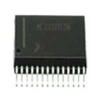
MC33742DW Freescale, MC33742DW Datasheet - Page 27

MC33742DW
Manufacturer Part Number
MC33742DW
Description
Manufacturer
Freescale
Datasheet
1.MC33742DW.pdf
(70 pages)
Specifications of MC33742DW
Data Rate
1000Kbps
Number Of Transceivers
1
Standard Supported
CAN 2.0
Operating Supply Voltage (max)
27V
Operating Supply Voltage (typ)
5/9/12/15/18/24V
Operating Supply Voltage (min)
4.5V
Package Type
SOIC W
Supply Current
45mA
Operating Temperature (max)
125C
Operating Temperature (min)
-40C
Operating Temperature Classification
Automotive
Mounting
Surface Mount
Pin Count
28
Lead Free Status / RoHS Status
Not Compliant
Available stocks
Company
Part Number
Manufacturer
Quantity
Price
Part Number:
MC33742DW
Manufacturer:
FREESCALE
Quantity:
20 000
Company:
Part Number:
MC33742DWR2
Manufacturer:
FREESCALE
Quantity:
8 845
SUPPLY VOLTAGE AT VSUP
pin. An external diode is needed in series with the VSUP pin
and the supply voltage to protect the SBC against negative
transients or from a reverse battery situation that can occur in
a vehicle application. The 33742 will operate from a supply
voltage input as low as 4.5VDC to as high as 27VDC. The
later voltage is often encountered during a vehicle jump-start.
such as load dump to 40V. The SBC is able to detect when
V
detected and retained in the parts Mode Control Register
(MCR) as the BATFAIL bit. This detection capability is
available across all operating modes.
mentioned in this section, refer to the section titled
Interface And Register Description
which provides a maskable interrupt if the VSUP voltage level
falls below 6.0V typical. Hysteresis is used to reduce false
detections. The early warning function works only in Normal
and Standby operation modes. An under-voltage at the
VSUP pin is reported in the Input / Output Register (IOR).
VDD REGULATOR
capable of supplying up to 200mA with monitoring circuitry for
under-voltage detection and a reset function. The VDD
regulator is protected against over-current and short-circuit
conditions. It has over-temperature detection and will set
warning flags (bit VDDTEMP in the MCR and INTR registers)
and has over-temperature shutdown with hysteresis.
V2 REGULATOR
voltage source The internal V2 circuitry will drive an external
series pass transistor, substantially increasing the available
supply current. Two pins, the V2 and the V2CTRL, are used
to sense and drive the series pass transistor. The output
INTRODUCTION
the SPI. The modes are Standby, Normal, Stop, and Sleep.
An additional temporary mode called Normal Request mode
is automatically accessed by the device after reset or wake-
up from Stop mode. A Reset mode is also implemented.
Special modes and configurations are possible for debug and
program microcontroller flash memory.
modes.
Analog Integrated Circuit Device Data
Freescale Semiconductor
SUP
The 33742 receives its operating voltage via the VSUP
The VSUP pin can tolerate automotive transient conditions
Note For a detailed description of all the registers
The SBC incorporates a V
The VDD regulator provides a 5.0V low dropout voltage
The V2 regulator feature provides for a second 5.0VDC
The 33742 has four modes of operation, all controllable via
Table
falls below 3.0V typical. This under-voltage state is
7, page 29, offers a summary of the functional
SUP
level early warning function,
beginning on page 47.
FUNCTIONAL DEVICE OPERATION
OPERATIONAL MODES
SPI
voltage is 5.0V and tracks the VDD regulator. The MJD32C
transistor is recommended for use as the external pass
device. Other PNP transistors can be used but depending on
the device’s gain, an external resistor-capacitor network
might be needed. V2 is also the supply voltage for the on-
board CAN module. An under-voltage condition for the V2
voltage is reported in the IOR Register (bit V2LOW set to
logic [1] if V2 falls below 4.0V typical).
HS VSUP SWITCH OUTPUT
pin. It can power or bias external switches and their
associated pullup or put-downs or other circuitry. An example
is biasing a set of switches connected to the L0 : L3 wake-up
input pins. The HS VSUP output current is limited to 200mA
and is protected against short circuits conditions and will
report an over-temperature shutdown condition (bit HSOT in
the IOR register and bit HSOT - V2LOW in the INTR register).
register. A cyclic mode of operation can be implemented
using an internal timer in the Sleep and Stop operating
modes. It can also be turned on in Normal or Standby modes
to drive loads or supply peripheral components. No internal
protection circuitry is provided, however. Dedicated chip
protection circuitry is required for inductive load applications.
The HS output pin should not go below - 0.3V.
BATTERY FAIL EARLY WARNING
Supply Voltage at VSUP.
INTERNAL CLOCK
timings (reset, watchdog, cyclic wake-up, filtering time, etc.).
There are two on-board oscillators: a higher accuracy (±12
percent) oscillator used in Normal Request, Normal, and
Standby modes, and a lower accuracy (±30 percent)
oscillator used during Sleep and Stop modes.
STANDBY MODE
regulator is turned OFF by disabling the V2CTRL pin. Other
functions available are the L0 : L3 inputs read through via the
SPI and HS output activation.
message is received, the CANWU bit is set. The watchdog
timer is running.
The HS output is a 2.0Ω typical switch tied to the VSUP
The HS output “on” state is set by the HSON bit in the IOR
Refer to the previous discussion under the heading,
The 33742 has an internal clock used to generate all
In Standby mode only the VDD regulator is ON. The V2
The CAN interface is not able to send messages. If a CAN
FUNCTIONAL DEVICE OPERATION
OPERATIONAL MODES
33742
27


