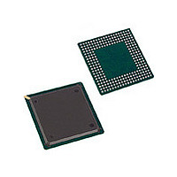
PXB4220EV3.4X Infineon Technologies, PXB4220EV3.4X Datasheet - Page 26

PXB4220EV3.4X
Manufacturer Part Number
PXB4220EV3.4X
Description
Manufacturer
Infineon Technologies
Datasheet
1.PXB4220EV3.4X.pdf
(290 pages)
Specifications of PXB4220EV3.4X
Data Rate
2.048Mbps
Number Of Channels
1
Operating Supply Voltage (typ)
3.3V
Operating Temp Range
-40C to 85C
Operating Temperature Classification
Industrial
Mounting
Surface Mount
Lead Free Status / RoHS Status
Compliant
- Current page: 26 of 290
- Download datasheet (4Mb)
Table 2
Pin No.
V5, Y4, Y3,
U5, V4
U9, Y8,
W8, V8,
Y7, W7,
V7, Y6
V9
W6
V6
Y9
Data Sheet
Symbol
RXADR[4:0]
TXDAT[7:0]
TXPTY
TXSOC
TXCLAV
TXCLK
UTOPIA Interface (36 pins) (cont’d)
Input (I)
Output (O)
I
PUA
I
PUA
I
PUA
I
PDA
Slave: O
Master: I
PDA
I
26
Function
UTOPIA Receive Address Bus
Five bit wide true data driven from the ATM
to MPHY layer to select the appropriate
MPHY device. RXADR[4] is the MSB.
UTOPIA Transmit Data Bus
Byte-wide true data driven from ATM to
PHY layer. TXDAT[7] is the MSB.
UTOPIA Transmit Odd Parity Bit
TXPTY is the odd parity bit over TXDAT[0:7]
driven by the ATM layer.
UTOPIA Transmit Start-of-Cell
Active high signal asserted by the ATM
layer when TXDAT[0:7] contains the first
valid byte of the cell.
UTOPIA Transmit Cell Available
Slave: TXCLAV is an active high signal
asserted by the PHY layer to indicate it can
accept data.
Master: TXCLAV is an active high signal
asserted by the ATM layer to indicate it can
accept data.
UTOPIA Transmit Clock
Data transfer/synchronization clock
provided by the ATM layer to the PHY layer
for synchronizing
PXB 4219E, PXB 4220E, PXB 4221E
transfers on
Pin Descriptions
TXDAT[0:7]
IWE8, V3.4
2003-01-20
.
Related parts for PXB4220EV3.4X
Image
Part Number
Description
Manufacturer
Datasheet
Request
R

Part Number:
Description:
IC CHIPSET 8 E1/T1 LINE 256-BGA
Manufacturer:
Infineon Technologies
Datasheet:

Part Number:
Description:
IC CHIPSET 8 E1/T1 LINE 256-BGA
Manufacturer:
Infineon Technologies
Datasheet:

Part Number:
Description:
Interworking Element for 8 E1/T1 Lines
Manufacturer:
Infineon Technologies AG
Datasheet:

Part Number:
Description:
members of Infineon ATM Chipset
Manufacturer:
Infineon Technologies AG
Datasheet:

Part Number:
Description:
Manufacturer:
Infineon Technologies AG
Datasheet:

Part Number:
Description:
Manufacturer:
Infineon Technologies AG
Datasheet:

Part Number:
Description:
Manufacturer:
Infineon Technologies AG
Datasheet:

Part Number:
Description:
Manufacturer:
Infineon Technologies AG
Datasheet:

Part Number:
Description:
Manufacturer:
Infineon Technologies AG
Datasheet:

Part Number:
Description:
Manufacturer:
Infineon Technologies AG
Datasheet:

Part Number:
Description:
Manufacturer:
Infineon Technologies AG
Datasheet:

Part Number:
Description:
16-bit microcontroller with 2x2 KByte RAM
Manufacturer:
Infineon Technologies AG
Datasheet:

Part Number:
Description:
NPN silicon RF transistor
Manufacturer:
Infineon Technologies AG
Datasheet:

Part Number:
Description:
NPN silicon RF transistor
Manufacturer:
Infineon Technologies AG
Datasheet:

Part Number:
Description:
NPN silicon RF transistor
Manufacturer:
Infineon Technologies AG
Datasheet:


