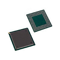
PXB4220EV3.4X Infineon Technologies, PXB4220EV3.4X Datasheet - Page 178

PXB4220EV3.4X
Manufacturer Part Number
PXB4220EV3.4X
Description
Manufacturer
Infineon Technologies
Datasheet
1.PXB4220EV3.4X.pdf
(290 pages)
Specifications of PXB4220EV3.4X
Data Rate
2.048Mbps
Number Of Channels
1
Operating Supply Voltage (typ)
3.3V
Operating Temp Range
-40C to 85C
Operating Temperature Classification
Industrial
Mounting
Surface Mount
Lead Free Status / RoHS Status
Compliant
- Current page: 178 of 290
- Download datasheet (4Mb)
7.24
Read/write Address 0001E
Reset value 1100
symn
rts_gen
rts_eval
bufthr
tfpp
rfpp
Data Sheet
bufthr0
15
7
Not used
Operation Mode Register (opmo)
tfpp
SYMn mode
This bit is relevant only in SYM2 and SYM8
0 =
1 =
RTS generation
0 =
1 =
RTS evaluation
0 =
1 =
Buffer threshold
Determines the threshold for the ATM Transmit Buffer. If the buffer level
remains under the threshold the signal ATBTC will be activated.
Transmit frame pulse polarity
valid for GIM
0 =
1 =
Receive frame pulse polarity
valid for GIM, SYM8 and SYM2
0 =
H
FRMFB[0] is used for frame and multiframe synchronization in
receive and transmit direction of all ports. FRMFB[1:7] are
unused
FRMFB[N] is used for frame and multiframe synchronization in
receive and transmit direction of corresponding ports
Pin SDI is used for RTS
RTS data are generated by ICRC
Pins FTCKO are used as transmit clock (all FTCKO[0:7] are input
pins)
Clock of ICRC is used as transmit clock and is also switched to
FTCKO pins (FTCKO[0:7] all are output pins)
FTMFS is active low
FTMFS is active high
FRMFB is active low
symn
rfpp
H
rts_gen
ftri
178
PXB 4219E, PXB 4220E, PXB 4221E
rts_eval
frri
om[1:0]
Register Description
bufthr[3:1]
IWE8, V3.4
2003-01-20
cbb
8
0
Related parts for PXB4220EV3.4X
Image
Part Number
Description
Manufacturer
Datasheet
Request
R

Part Number:
Description:
IC CHIPSET 8 E1/T1 LINE 256-BGA
Manufacturer:
Infineon Technologies
Datasheet:

Part Number:
Description:
IC CHIPSET 8 E1/T1 LINE 256-BGA
Manufacturer:
Infineon Technologies
Datasheet:

Part Number:
Description:
Interworking Element for 8 E1/T1 Lines
Manufacturer:
Infineon Technologies AG
Datasheet:

Part Number:
Description:
members of Infineon ATM Chipset
Manufacturer:
Infineon Technologies AG
Datasheet:

Part Number:
Description:
Manufacturer:
Infineon Technologies AG
Datasheet:

Part Number:
Description:
Manufacturer:
Infineon Technologies AG
Datasheet:

Part Number:
Description:
Manufacturer:
Infineon Technologies AG
Datasheet:

Part Number:
Description:
Manufacturer:
Infineon Technologies AG
Datasheet:

Part Number:
Description:
Manufacturer:
Infineon Technologies AG
Datasheet:

Part Number:
Description:
Manufacturer:
Infineon Technologies AG
Datasheet:

Part Number:
Description:
Manufacturer:
Infineon Technologies AG
Datasheet:

Part Number:
Description:
16-bit microcontroller with 2x2 KByte RAM
Manufacturer:
Infineon Technologies AG
Datasheet:

Part Number:
Description:
NPN silicon RF transistor
Manufacturer:
Infineon Technologies AG
Datasheet:

Part Number:
Description:
NPN silicon RF transistor
Manufacturer:
Infineon Technologies AG
Datasheet:

Part Number:
Description:
NPN silicon RF transistor
Manufacturer:
Infineon Technologies AG
Datasheet:


