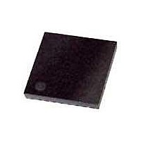
ATA5811-PLQW80 Atmel, ATA5811-PLQW80 Datasheet - Page 30

ATA5811-PLQW80
Manufacturer Part Number
ATA5811-PLQW80
Description
RF Transceiver RF Data Control Transceiver
Manufacturer
Atmel
Datasheet
1.ATA5811-PLHC.pdf
(92 pages)
Specifications of ATA5811-PLQW80
Wireless Frequency
226 KHz
Interface Type
4-Wire SPI
Noise Figure
7 dB
Output Power
10 dBm
Operating Supply Voltage
2.4 V to 5.25 V
Maximum Operating Temperature
+ 105 C
Mounting Style
SMD/SMT
Package / Case
QFN-48
Maximum Data Rate
20 Kbps
Minimum Operating Temperature
- 40 C
Modulation
ASK, FSK
Lead Free Status / RoHS Status
Lead free / RoHS Compliant
7.2
7.3
7.4
30
AUX Mode
Idle Mode
Reset Timing and Reset Logic
ATA5811/ATA5812
The transceiver changes from OFF mode to AUX mode if the voltage at pin VAUX V
(typically). In AUX mode DVCC and VSOUT are connected to the auxiliary power supply input
(VAUX) via the voltage regulator V_REG2. In AUX mode the transceiver is programmable via
the 4-wire serial interface, but no RX or TX operations are possible because AVCC = OFF.
The state transition OFF mode to AUX mode is indicated by an interrupt at pin IRQ and the sta-
tus bit P_On_Aux = 1.
In Idle mode AVCC and DVCC are connected to the battery voltage (VS1).
From OFF mode the transceiver changes to Idle mode if pin PWR_ON is set to 1 or pin T1, T2,
T3, T4 or T5 is set to 0. This state transition is indicated by an interrupt at pin IRQ and the status
bits Power_On = 1 or ST1, ST2, ST3, ST4 or ST5 = 1.
From AUX mode the transceiver changes to Idle mode by setting AVCC_EN = 1 in control
register 1 via the 4-wire serial interface or if pin PWR_ON is set to 1 or pin T1, T2, T3, T4 or T5
is set to 0.
VSOUT is either connected to VS1 or to the auxiliary power supply (V_REG2).
If V
nected to V_REG2 and the status bit P_On_Aux is set to 1.
In Idle mode the RF transceiver is disabled and the power consumption I
(VSOUT OFF and CLK output OFF VS1 = VS2 = 3V). The exact value of this current is strongly
dependent on the application and the exact operation mode, therefore check the section
cal Characteristics: General” on page 63
Via the 4-wire serial interface a connected microcontroller can program the required parameter
and enable the TX, RX polling or RX mode.
The transceiver can be set back to OFF mode by an OFF command via the 4-wire serial inter-
face (the bit AVCC_EN must be set to 0, the input level of pin PWR_ON must be 0 and pin T1,
T2, T3, T4 and T5 = 1 before writing the OFF command).
Table 7-1.
If the transceiver is switched on (OFF mode to Idle mode, OFF mode to AUX mode) DVCC and
VSOUT are ramping up as illustrated in
ceiver is set to the Idle mode). The internal signal DVCC_RESET resets the digital control logic
and sets the control register to default values.
A voltage monitor generates a low level at pin N_RESET until the voltage at pin VSOUT
exceeds 2.38V (typically) and the start-up time of the XTO has elapsed (amplitude detector, see
Figure 6-2 on page
time of the XTO has elapsed the output clock at pin CLK is available. Because the enabling of
pin CLK is asynchronous the first clock cycle may be incomplete.
VAUX
< VS1 + 0.5V, VSOUT is connected to VS1. If V
OPM1
Control Register 1
0
25). After the voltage at pin VSOUT exceeds 2.3V (typically) and the start-up
Figure 7-3 on page 31
for the appropriate application case.
OPM0
0
VAUX
(AVCC only ramps up if the trans-
> V
S1
+ 0.5V, VSOUT is con-
S_IDLE
Idle mode
Function
is about 230 µA
4689F–RKE–08/06
VAUX
“Electri-
> 3.5V


